
In hardware design, engineers often dedicate 90% of their focus to routing, impedance, and stack-ups, while overlooking the thin layer of ink covering the copper: the PCB solder mask. This layer does more than determine the board's aesthetics. It directly impacts SMT assembly yield, pad insulation, and long-term product reliability. Today, from the perspective of AnyPCBA's manufacturing and DFM review team, we break down the engineering essentials behind solder mask design.
1. What is a PCB Solder Mask & Why is it Mostly Green?
The solder mask (also known as solder resist) is a photosensitive polymer ink applied to the PCB surface. Its core purposes are threefold:
Prevent Short Circuits: Stops solder from flowing to unintended areas during assembly.
Protect Copper: Isolates copper traces from air and moisture, preventing oxidation and chemical corrosion.
Electrical Insulation: Provides a reliable insulating barrier for high-density routing.
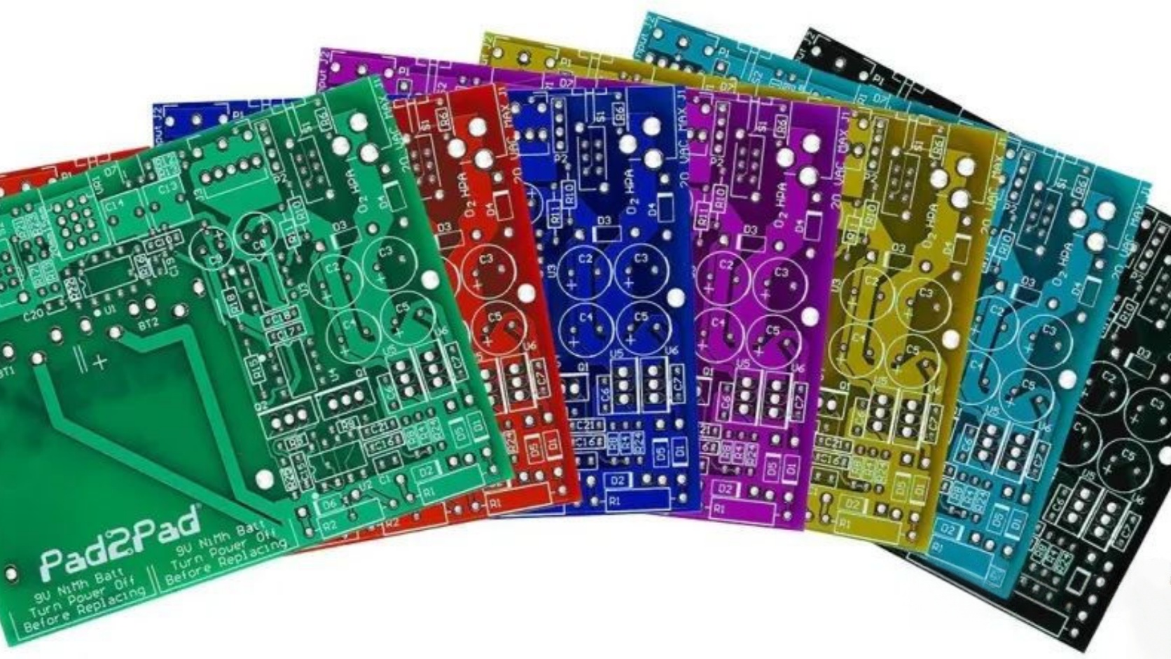
Although solder mask can technically be red, black, blue, or white, over 90% of circuit boards worldwide default to green. This is because:
Mature Process: Green ink has the most stable formulation, highest procurement volume, and lowest cost.
Manufacturing Friendly: During SMT and AOI (Automated Optical Inspection), the green background provides the highest contrast against silver solder joints and gold pads, maximizing machine vision recognition rates.
High Resolution: Green ink achieves higher resolution during exposure and development, making it ideal for creating ultra-fine solder bridges.
2. Crucial DFM Rules: Solder Bridge (Solder Bridge) Design
During DFM reviews, we frequently see beginners overlook solder bridges when designing dense IC footprints.
What is a solder bridge? It is the thin strip of solder mask between two adjacent pads. Its purpose is to block solder from flowing laterally during reflow soldering, preventing adjacent IC pins from short-circuiting (solder bridging).
AnyPCBA DFM Tips: Many factories take the easy route: if the client doesn't specify, they simply remove the solder mask between fine-pitch pins (e.g., 0.5mm QFN or QFP), creating a continuous opening. This introduces severe short-circuit risks.
At AnyPCBA, our DFM team checks your solder bridge widths based on copper thickness and mask color:
Standard Green Ink: Solder bridge width is recommended to be ≥ 3 mil (minimum 2.5 mil). For other colors, ≥ 4 mil is recommended.
Large Copper Areas: In large copper pour areas, to prevent solder bridging, the solder dam must be ≥ 8 mil.
Opening Clearance: Generally, the solder mask opening should have a single-side clearance of ≥ 2.0 mil.
3. Why Do Vias Need Solder Mask Tenting / Plugging?
In HDI or dense BGA areas, you will see vias completely filled with green ink, making them opaque. This is known as via tenting or via plugging.
For high-density assemblies, via plugging offers four major advantages:
Prevent Short Circuits: For vias under BGAs, if not plugged, solder can easily wick through the via to the other side, causing fatal shorts.
Avoid Cold Joints: During SMT, if a via is not properly plugged, solder paste can flow into the hole, leaving insufficient solder on the pad and causing weak joints.
Prevent Flux Residue: During wave soldering, plugging prevents flux from entering the via, avoiding long-term corrosion.
Enable Vacuum Pick-up: A flat surface is necessary for automated equipment using vacuum suction during testing and packaging.
Note: Generally, vias with a finished diameter below 0.16mm can be perfectly tented. AnyPCBA supports high-density via plugging processes, ensuring flat, opaque via holes.
4. Solder Mask vs. Paste Mask: Don't Mix Them Up
When exporting Gerber files, many engineers confuse the Solder Mask with the Paste Mask.
Solder Mask: It is a negative film. Where you draw the shape, there is NO solder mask (copper is exposed for soldering or testing). The undrawn areas are covered in mask.
Paste Mask: Used for SMT stencil openings. Its size usually matches the SMT pads exactly or with slight adjustments. The stencil uses this layer to print solder paste onto the pads.
5. AnyPCBA's Solder Mask Acceptance Standards
To ensure your design lands perfectly, AnyPCBA strictly controls solder mask processes according to IPC-SM-840C and higher standards:
Thickness Requirements: For Class 2 products, the minimum solder mask thickness is 10μm; for Class 3 (high reliability) products, it must reach at least 18μm.
Via Requirements: Vias designated for mask coverage must absolutely prevent ink from bleeding into the hole or allowing light to pass through.
Surface Flatness: No bubbling, wrinkling, scratching, exposed copper, or obvious uneven imprinting is permitted.
Gold Finger Protection: Gold fingers must absolutely be free of any ink contamination to ensure reliable insertion and contact.
Conclusion
Though it is just a thin layer of ink, the solder mask plays a decisive role in preventing short circuits and ensuring SMT yield. Before your next prototype run, consider sending your Gerbers to AnyPCBA. Our DFM team provides free, professional reviews of your solder bridges and via processes, helping you eliminate short-circuit risks before manufacturing even begins.