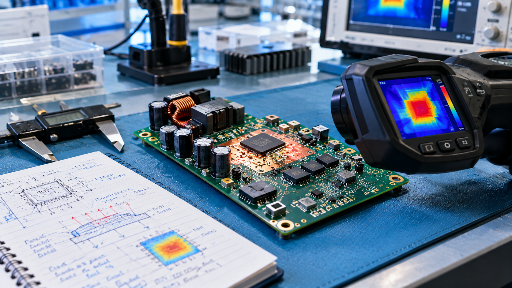
Excessive temperature rise in power chips is a common headache for engineers. PCB thermal optimization is one of the most effective ways to reduce chip temperature. This guide outlines the core principles and practical techniques for PCB heat dissipation.
"Energy can neither be created nor destroyed" — this is the law of conservation of energy, and heat is no exception.
A chip's temperature is a manifestation of heat. If heat is concentrated in a narrow space, temperature rises. If it is spread over a larger area, temperature drops.
To optimize PCB heat dissipation, you must first understand two things:
Where is the heat generated?
Through what paths does the heat dissipate?
Chip heat is primarily generated on the internal die. There are two main heat conduction paths:
This is the path where heat dissipates through the top of the package. Resin packaging has relatively low thermal conductivity, so this path is less efficient.
Inside the IC, because metal has much higher thermal conductivity than resin packaging, most heat is transferred out through metal pins or thermal pads. This is the core path for PCB thermal optimization.
Key conclusion: Optimizing PCB heat dissipation is essentially about optimizing the efficiency of the "die → metal pins/thermal pad → PCB → air" heat conduction path.
During the initial PCB layout phase, avoid concentrating multiple heat sources (such as multiple power chips, power MOSFETs, high-power MCUs) in one local area of the board. This leads to heat accumulation.
What to do: Leave spacing between heat sources so heat is distributed more evenly across the board.
When designing component footprints, follow recommended pad design rules and provide slightly more area than the chip pin itself.
Why? If the package pin pad area is small, after soldering, the contact area between solder, pin, and PCB is small — resulting in poor thermal conduction and a higher risk of cold solder joints. If the pad area is appropriately larger, the solder joint has greater contact area with both the pin and the PCB, improving thermal conduction.
To improve PCB heat dissipation, increase the copper pour area for power and ground traces, allowing heat to transfer more quickly.
Key design points:
Prioritize the top and bottom layers for power traces or ground planes
Increase copper pour area to assist heat dissipation
For multilayer boards, the top and bottom layers typically use 1oz copper, while inner layers use 0.5oz — so top and bottom layer copper has higher thermal conductivity than inner layers
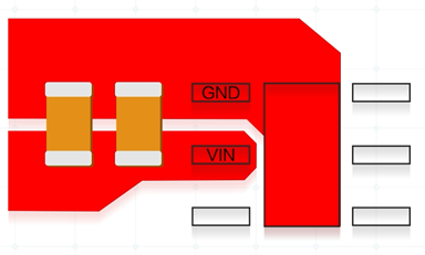
Why are top and bottom layers better for heat dissipation? Because they are closer to the air, making it easier for heat to dissipate.
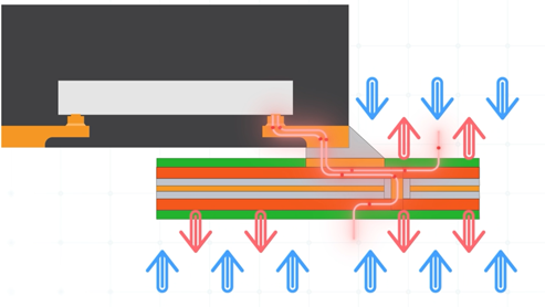
If an inner layer is used as a large copper pour, heat must first pass through the inner copper, then through the insulating layers and top/bottom copper before reaching the air — making it harder for heat to dissipate and causing chip temperatures to rise. Therefore, ground copper pour strategy is critical.
If the PCB process allows, increasing copper thickness provides a larger cross-sectional area, enhancing the thermal conductivity of PCB traces.
Different PCB layers use different copper thicknesses, resulting in different thermal conductivity.
Typical multilayer board structure:
Top and bottom layers: 1oz copper
Inner layers: 0.5oz copper
Therefore, prioritize routing critical thermal paths on the top or bottom layers, taking advantage of thicker copper and proximity to air.
Adding thermal vias is one of the most direct ways to improve heat dissipation.
Design points:
Generally, more thermal vias improve heat conduction
Larger via diameters improve heat conduction
Within reasonable limits, increase both the number and diameter of thermal vias
Thermal vias are typically placed evenly on the thermal pad, directly beneath the chip, or near power pins, allowing heat to transfer quickly to the large copper plane on the bottom layer and making PCB heat dissipation more uniform
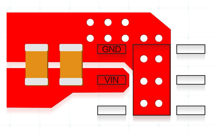
Provided product insulation reliability is maintained, solder mask can be removed on the bottom layer directly beneath the IC or at thermal via locations, exposing bare copper. This reduces thermal resistance between copper and air, improving heat dissipation.
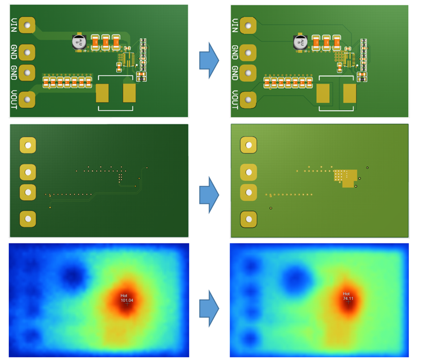
DCDC power chip MPQ8633B, using a 4-layer PCB, with component positions unchanged, improving PCB layout design:
Improvements:
Increased pin contact area
Increased power trace copper pour
Changed from inner-layer large ground pour to top and bottom layer large ground pour
Increased thermal via count and diameter
Exposed copper on the bottom layer
Test results:
Both PCB layouts were tested at 25°C ambient temperature with the same full load for 10 minutes. The measured IC surface temperatures were 101°C and 74°C, respectively.
Conclusion: By optimizing copper pour layers, increasing thermal vias, and exposing bottom copper, the IC surface temperature was reduced by 27°C — a significant thermal improvement.
| # | Technique | Description |
|---|---|---|
| 1 | Leave spacing between heat sources | Avoid concentrated placement, balance heat distribution |
| 2 | Make pin pads slightly larger than pins | Ensure sufficient solder contact area for thermal conduction |
| 3 | Prioritize top/bottom layers for power/ground | Larger copper pour area, closer to air for heat dissipation |
| 4 | Increase copper thickness if process allows | Larger cross-sectional area for better heat conduction |
| 5 | Add thermal vias and use bottom-layer copper | Expose copper when necessary to reduce thermal resistance |
The core of PCB thermal optimization is understanding where heat is generated and how it conducts, then optimizing each step of the path:
Layout: Distribute heat sources to avoid local hotspots
Pads: Increase contact area for better thermal conduction
Copper pour: Prioritize top/bottom layers, increase area
Copper thickness: Increase when process allows
Thermal vias: Balance quantity and diameter, distribute evenly
Exposed copper: Reduce thermal resistance between copper and air
Need PCB Thermal Design or Manufacturing Support?
AnyPCBA's engineering team focuses on thermal management, copper pour strategy, and thermal via design during design reviews. Whether you're working on power modules or high-power-density boards, we provide DFM/DFA design reviews to identify potential thermal issues before fabrication.
Our manufacturing capabilities cover 2-64 layers, including HDI, rigid-flex, heavy copper, and metal-core PCB processes.
Contact us to discuss your project →




