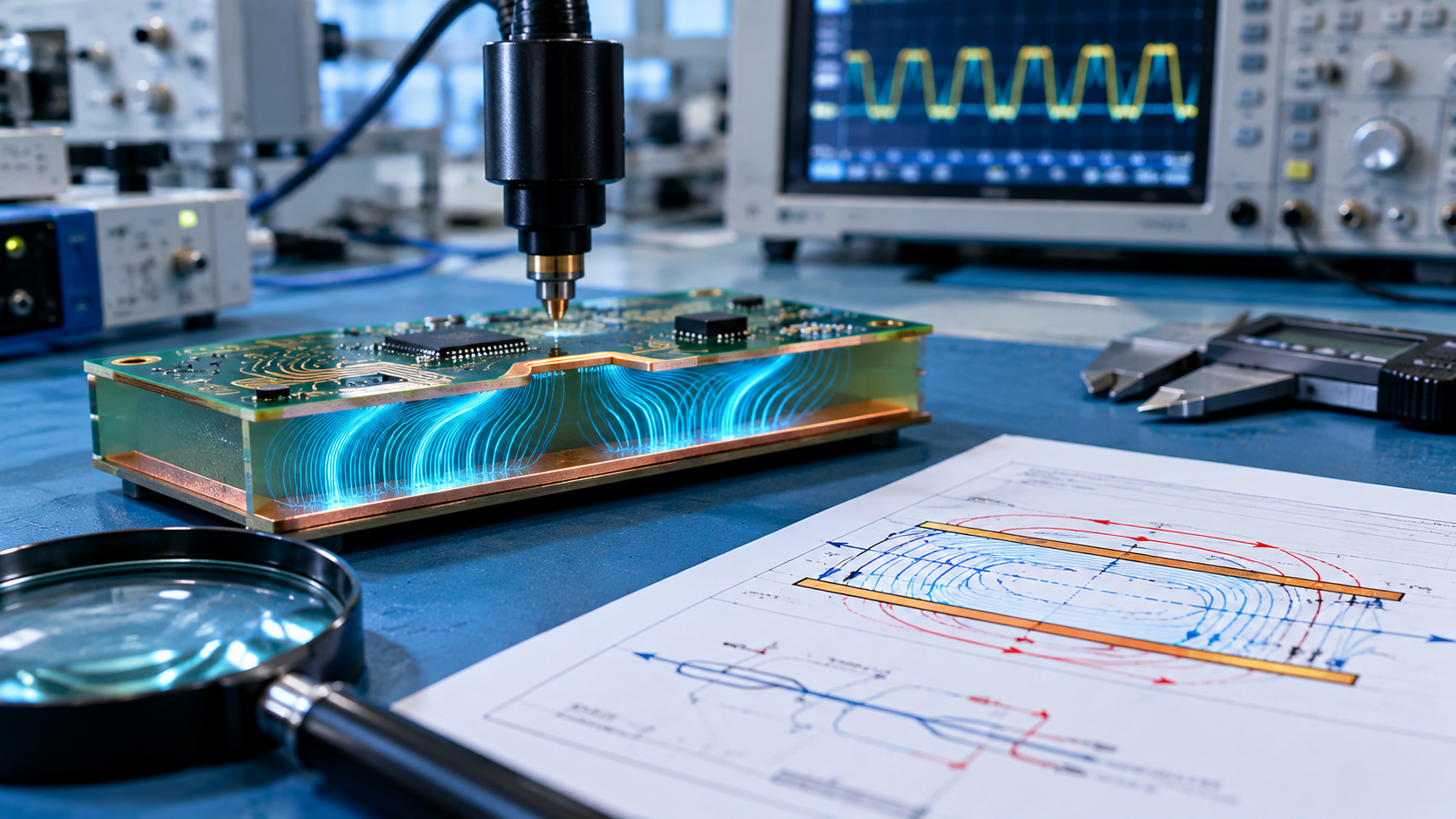
When designing a printed circuit board (PCB) for electromagnetic compatibility (EMC), it's essential to understand signal propagation from the perspective of electromagnetic fields and current. These concepts matter because they help us design PCBs with low electromagnetic radiation and low sensitivity to external radiation or interference.
This article explores the core concepts of signal propagation in PCBs and explains how to apply them in practical board design.
When thinking about how signals travel in a PCB, you need to shift from the analogy of "water flowing through a pipe" to thinking in terms of electromagnetic fields and transmission lines.
A transmission line is a structure designed to transfer energy from one point to another in the form of a confined electromagnetic field. In a PCB, a transmission line consists of at least two conductors — both are equally important in confining the electromagnetic field and guiding it from one point in the circuit to another. Without one of the conductors, the electromagnetic field that makes up the signal cannot be confined, and the spread of these fields can lead to EMC test failures.
This leads to a very important concept: the electromagnetic signal is not contained inside the conductor, but exists in the dielectric between the two conductors and the surrounding space. From an EMC perspective, our goal is to maximize the confined electromagnetic field between the two conductors and reduce the electromagnetic field around them.
In a PCB, the two conductors used for signal propagation are the signal potential conductor and the return and reference potential conductor. The most intuitive example is a two-layer board:
Top layer: Connects to the signal source, used for routing signal traces
Bottom layer: Solid copper plane, connects to the signal source and also to the signal potential reference
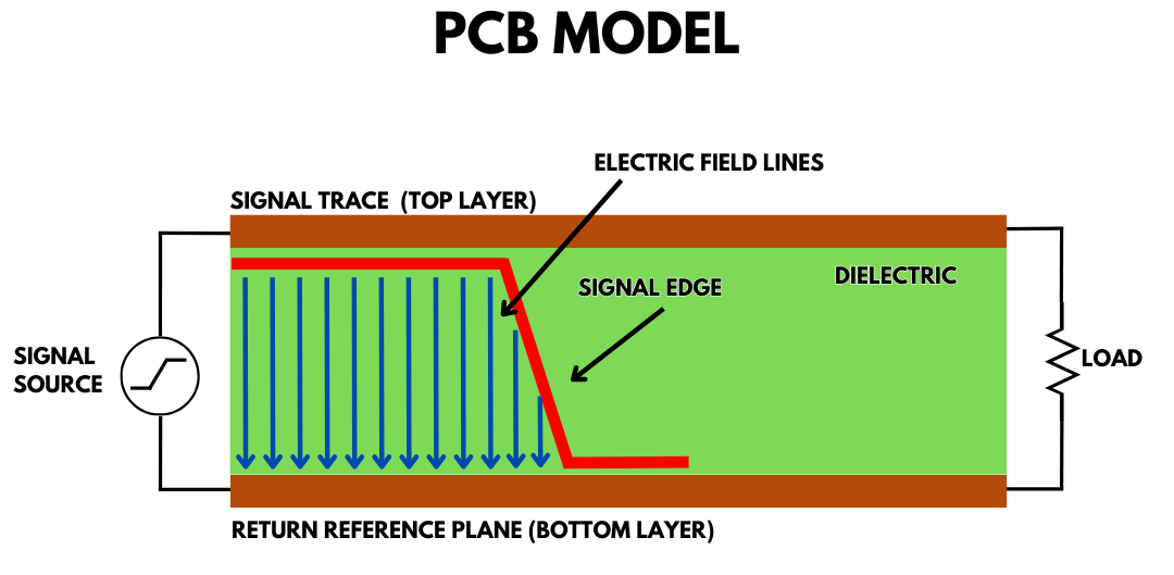
What we call the "signal" is actually the electromagnetic field between these two conductors — meaning the signal does not exist in a single conductor, but rather as electromagnetic energy in the dielectric between the two conductors.
This also shows that the properties of the dielectric material affect signal propagation, particularly the speed of signal (or electromagnetic wave) propagation — the speed of light in the dielectric. Between the two conductors, there will be points where the signal has arrived and points where it has not. In digital signals, the transition point between the signal region and the no-signal region is called the signal edge or signal wavefront — the transition point where the digital logic level goes from low to high.
From an EMC perspective, this transition point is critical because it is where the electric and magnetic fields between conductors change from low to high. The faster the energy state changes — that is, the faster the signal transitions from low to high logic level — the greater the energy change compressed into a short time. When the signal propagates from source to destination in the transmission line, the signal wavefront or signal edge guides the signal's propagation.
Another important concept: when the signal edge propagates, because the leading edge is a change in the electromagnetic field, this generates displacement current in the dielectric between the two conductors. This phenomenon is explained by Maxwell's equations (particularly the Ampère-Maxwell law).
The most intuitive way to understand this is to imagine the current flow when an AC source is applied to a capacitor.
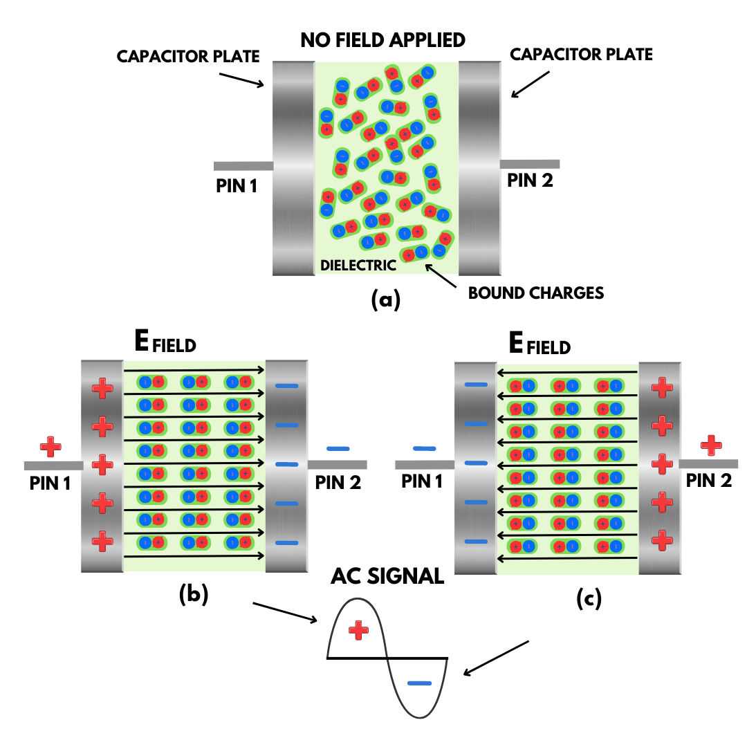
In reality, there is no conduction current between the capacitor plates and the dielectric, but the bound charges in the dielectric undergo polarization (displacement) in response to the electric field applied by the plates. This looks like conduction current flowing through the capacitor plates.
The concept of displacement current is important because it explains how current forms during signal propagation, especially before reaching the load. Classical circuit theory states that current always flows in loops. So why does current exist before the signal reaches the load, before a continuous conduction current loop from source to load and back is established? This is precisely due to the existence of displacement current, which allows current to still flow in a loop during signal propagation.
If there were only conduction current and no displacement current, the signal could not propagate — because a current loop consisting only of conduction current cannot close before reaching the load. This means conduction current would have to flow through the dielectric, which is impossible by definition. But with displacement current — an "apparent current" — the loop closes instantaneously as the signal propagates.
The combination of conduction current and displacement current forms a current loop that propagates with the signal edge. This current loop can be divided into three parts:
| Current Type | Path | Description |
|---|---|---|
| Forward Current | In the top-layer conductor toward the load | Along the signal direction |
| Return Current | In the bottom-layer conductor back to the source | Opposite to the signal direction |
| Displacement Current | Through the dielectric between conductors | Follows the signal edge, bridging the other two parts |
Managing the confinement of electromagnetic fields between conductors and controlling current paths is critical for designing PCBs that are not only high-performance but also excellent in electromagnetic compatibility and signal integrity.
Core Principles:
Maximize confined electromagnetic fields: Ensure signal traces have closely adjacent reference planes, concentrating the electromagnetic field between the trace and the plane
Minimize radiated electromagnetic fields: Reduce stray fields around traces to lower EMI radiation
Control return current paths: Ensure return current flows directly beneath the signal trace, minimizing loop area
Maintain reference plane integrity: Avoid splits or slots that force return current to detour
This approach allows us to control radiation at the source and avoid designing PCB structures that allow external interference coupling.
Understanding this explains why dielectric material selection (Dk/Df) is so important for high-speed signals. Material properties directly affect signal propagation speed and loss.
Signal current and return current together form a loop. If the return path is discontinuous, signal integrity degrades. This is why reference plane integrity is critical.
This is a fundamental but often overlooked concept. Displacement current closes the loop instantaneously during signal propagation, ensuring normal signal transmission.
Rather than fixing failures after testing, it's better to control electromagnetic field confinement and current paths at the design stage. This includes:
Ensuring signal traces have complete reference planes
Avoiding routing across plane splits
Controlling trace length and loop area
Selecting appropriate dielectric materials
Signal propagation in a PCB is fundamentally the propagation of electromagnetic fields between conductors and dielectric. Understanding this physical nature is the foundation of good EMC design.
Key Takeaways:
Signals are electromagnetic fields between conductors, not current inside a conductor
Transmission lines require two conductors (signal + return) to confine the electromagnetic field
Displacement current explains how the current loop closes during signal propagation
Confining fields and controlling current paths is key to EMI control
Dielectric material properties directly affect signal propagation speed and loss
Need Low-EMI PCB Design or Manufacturing Support?
AnyPCBA's engineering team focuses on electromagnetic field confinement, current path control, and reference plane integrity during design reviews. Whether you're working on high-speed digital circuits or mixed-signal systems, we provide DFM/DFA design reviews to identify potential EMI risks before fabrication.
Our manufacturing capabilities cover 2-64 layers, including HDI, rigid-flex, and high-frequency hybrid processes.
Contact us to discuss your project →




