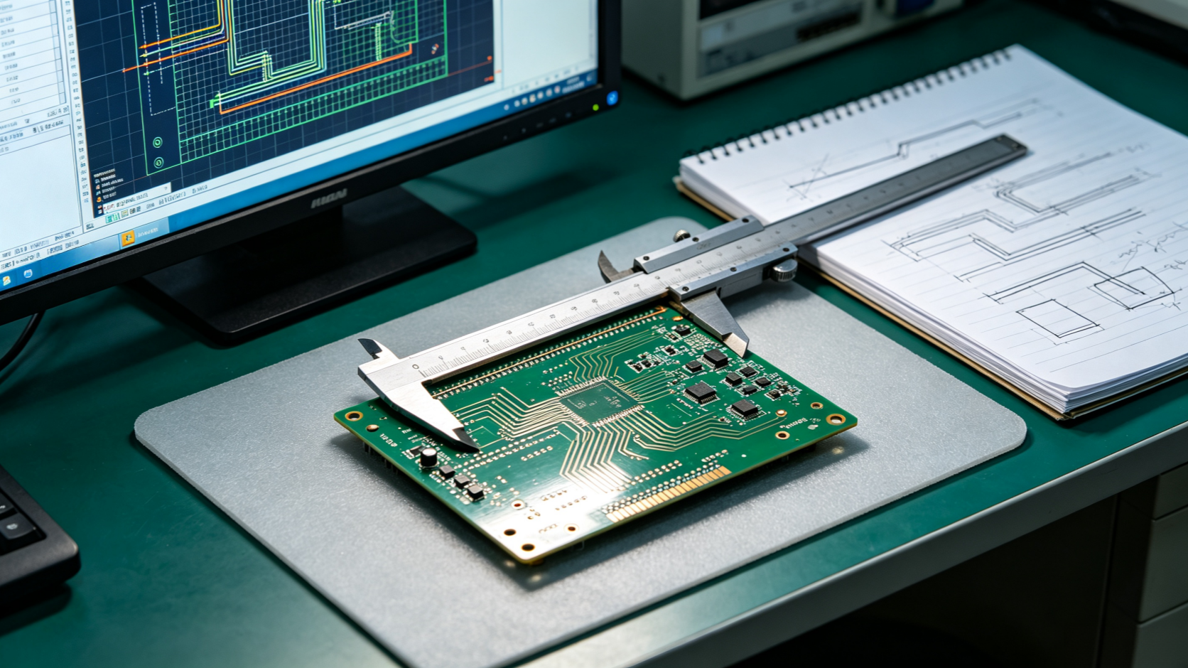
For beginner engineers and PCB design newcomers, mastering PCB design guidelines is essential. This guide breaks down common PCB design rules and manufacturer requirements, and provides an overview of the key fundamentals.
Basic PCB design guidelines include controlling current capacity and impedance — critical for preventing arcing and crosstalk. Additionally:
Select appropriate via types, considering aspect ratio, covering, and plugging to ensure reliability
Choose materials and layer arrangements that improve signal integrity, thermal performance, and manufacturability
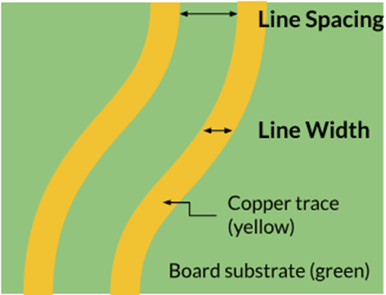
Trace width and spacing affect current-carrying capacity, impedance, and board density.
Trace Width: Determines the current capacity a trace can safely carry without generating excessive heat. Power and ground traces are wider; signal traces are narrower.
Trace Spacing: The distance between adjacent traces must be sufficient to prevent arcing and crosstalk — especially in high-frequency designs.
| Factor | Description |
|---|---|
| Current Requirements | Use IPC-2152 guidelines to calculate the appropriate trace width for expected current |
| Impedance Control | For high-speed signals, precise trace widths are needed to maintain characteristic impedance |
| Manufacturing Limits | Manufacturers have process limits on minimum trace width/spacing — standard processes typically around 0.075mm (3 mil) |
An annular ring is the copper ring surrounding a plated via in a PCB, ensuring reliable electrical connection between layers.
Minimum Annular Ring: The minimum allowable width of the ring to ensure structural integrity and electrical reliability.
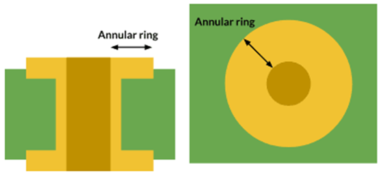
Design for Manufacturability: Consider drill offset and registration tolerances to prevent the drill from encroaching on the pad edge and causing breakout.
Standard guidelines recommend a minimum annular ring width of 0.05mm to 0.1mm, though the specific value may vary depending on manufacturing capabilities and board requirements.
Solder mask is a protective layer that prevents solder bridging and protects copper traces from environmental exposure.
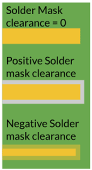
Solder mask clearance refers to the intentional gap between the solder mask and the surrounding pad or trace.
| Type | Description |
|---|---|
| Positive Clearance | Exposes more pad area — suitable for hand soldering |
| Negative Clearance | Covers more of the pad — prevents solder wicking |
| Solder Mask Dam | Narrow strip of solder mask between closely spaced pads — prevents shorts between fine-pitch component pins |
Key Design Points:
Standard manufacturing tolerances allow solder mask to extend 0.05mm to 0.075mm beyond the copper feature
Select solder mask openings based on component size, component type, and assembly method
Vias are used to establish electrical connections between different PCB layers. Via types include:
| Type | Description |
|---|---|
| Through-Hole Via | Extends from top layer to bottom layer |
| Blind Via | Connects outer layer to one or more inner layers |
| Buried Via | Connects inner layers without reaching the surface |
Factors to consider when selecting vias:
Aspect Ratio: The ratio of PCB thickness to via diameter, affecting manufacturability. Lower aspect ratios (< 10:1) are recommended.
Via Covering and Plugging: Additional features that determine via function.
Covering: Using solder mask to cover the via, preventing contamination
Plugging: Filling the via with resin or conductive material for reliability in high-density designs
Designers should specify via sizes and types that meet both electrical requirements and manufacturing capabilities.
Selecting appropriate materials and defining the layer stackup is key to ensuring overall board functionality and reliability.
| Parameter | Description |
|---|---|
| Base Material | FR-4 is typical, but Rogers and other alternatives may be used for high-frequency applications |
| Dielectric Constant | Affects signal speed and impedance calculations |
| Layer Count | Determined by circuit complexity and routing density |
Design specifications should clearly define:
Material Type: Indicate flame retardant rating and thermal performance if needed
Thickness: Dielectric and copper foil thickness
Layer Stackup Order: Arrange signal, power, and ground layers to optimize performance
The choice of surface finish affects solderability, service life, and cost.
| Finish | Characteristics |
|---|---|
| HASL (Hot Air Solder Leveling) | Lower cost, but uneven surface — not suitable for fine-pitch components |
| ENIG (Electroless Nickel Immersion Gold) | Flat surface, excellent solderability — but higher cost |
| OSP (Organic Solderability Preservative) | Cost-effective, but limited shelf life |
Designers should choose the most appropriate surface finish based on assembly requirements and budget constraints.
Copper thickness refers to the thickness of the copper layers in a PCB, typically measured in ounces per square foot (oz/ft²). Standard thicknesses range from 1 oz/ft² (35μm) to 2 oz/ft² (70μm), though other values can be specified based on current-carrying requirements.
| Parameter | Description |
|---|---|
| Current Capacity | Thicker copper layers carry higher currents without excessive heat buildup |
| Thermal Management | Increased copper thickness also improves board heat dissipation |
Planes are copper areas used for power and ground, providing low-resistance paths and effective heat dissipation. Plane clearance refers to the spacing between the plane and other unconnected conductive elements, such as vias passing through the plane.
| Consideration | Description |
|---|---|
| Electrical Isolation | Sufficient clearance prevents short circuits and electrical interference between different nets |
| Manufacturing Tolerance | Etching tolerances must be considered during PCB fabrication to avoid accidental connections |
| Regulatory Compliance | Safety standards may specify minimum clearances, especially for high-voltage applications |
Designers should set clearance based on electrical requirements and manufacturing capabilities, typically between 0.2mm and 0.5mm, but adjustable based on specific constraints.
If the board requires high-speed or high-power components, further design guidelines should be applied.
In high-speed and high-frequency circuits, controlled impedance is required to maintain signal integrity.
| Parameter | Description |
|---|---|
| Trace Geometry | Trace width, thickness, and relative spacing to reference planes determine impedance |
| Dielectric Stackup Configuration | Beyond layer arrangement, PCB substrate properties also affect signal propagation |
Design specifications should include:
Impedance Tolerance: Typically ±10%, but tighter tolerances may be required in critical applications
Impedance Coupons: Include in the design to verify impedance during manufacturing
Effective thermal management ensures long-term service life and operational reliability of electronic components.
Thermal management measures:
Set up dedicated layers or areas to dissipate heat generated by high-power components
Form thermal via arrays to conduct heat to inner layers or the opposite side of the PCB
Consider metal-core PCBs or other high-thermal-conductivity substrates to improve heat dissipation
Thermal relief pads: Consist of thin traces (spokes) connecting the pad to the plane, effectively reducing heat conduction into the copper plane and ensuring the pad heats up evenly during soldering. By controlling heat flow, these pads help ensure proper component soldering, preventing cold solder joints that compromise connection reliability.
Designers can adjust the number and width of thermal relief spokes based on the thermal characteristics of the board and components. Using thermal relief pads not only improves soldering but also enhances overall PCB reliability, especially in designs with large copper areas.
From basic trace width and spacing to advanced controlled impedance and thermal management, PCB design guidelines run through the entire design process. For beginner engineers, mastering these fundamentals is the prerequisite for ensuring a design is manufacturable, reliable, and high-performance.
Key Takeaways:
Trace Width and Spacing: Determine current capacity, impedance, and density
Annular Ring: Ensures via reliability — minimum width 0.05–0.1mm
Solder Mask Clearance: Positive, negative, and dams serve different purposes
Via Types: Through-hole, blind, buried — consider aspect ratio
Materials and Stackup: FR-4 or Rogers; layer order affects performance
Surface Finish: HASL, ENIG, OSP each have trade-offs
Copper Thickness: 1–2 oz/ft² standard; affects current and heat
Plane Clearance: 0.2–0.5mm for electrical isolation
Thermal Relief: Improves soldering reliability, especially with large copper areas
Need PCB Design or Manufacturing Support?
AnyPCBA's engineering team focuses on trace width, annular rings, via design, material selection, and surface finish during design reviews. Whether you're a beginner or an experienced designer, we provide DFM/DFA design reviews to help you identify potential design issues before fabrication.
Our manufacturing capabilities cover 2-64 layers, including HDI, rigid-flex, and high-frequency hybrid processes.
Contact us to discuss your project →




