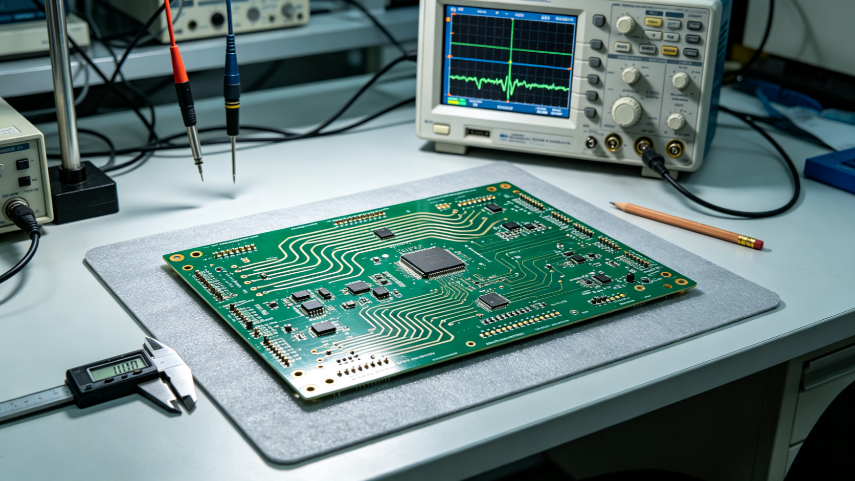
According to industry statistics, over 60% of hardware rework originates from signal reflection, crosstalk, or timing skew. Traditional design methods that rely heavily on simulation are often time-consuming and costly. This guide presents 7 field-verified routing topology strategies that can achieve up to 90% signal quality improvement without deep simulation — particularly useful for DDR, PCIe, and SerDes high-speed scenarios.
Application: PCIe / USB ultra-high-speed signals
Key Requirements:
Path length mismatch < 5 mil
Via count ≤ 1
Constant differential pair spacing
Why It Works: Point-to-point routing eliminates impedance discontinuities and reflections caused by branches — the simplest and most effective topology. For PCIe Gen4/5 and similar ultra-high-speed signals, any branch creates significant signal reflection.
Additional Tip: If vias are unavoidable, use back-drilling to remove stubs. Keep stub length below 4 mil.
Application: I²C / SPI / CAN
Key Requirements:
Branch length mismatch < 50 mil
Add 1 kΩ pull-up resistor at the far end
Why It Works: Daisy chain topology allows the signal to pass through each device sequentially — suitable for low-speed buses. At lower speeds, reflection effects from branches have relatively less impact on signal integrity.
Additional Tip: For I²C buses, pull-up resistor selection must balance rise time and power consumption. Calculate optimal resistance based on bus capacitance — typically between 1 kΩ and 10 kΩ.
Application: Multi-load buses (e.g., RGB LED drivers)
Key Requirements:
Main trunk width +20%
Branch length mismatch < 2 mil
Why It Works: Star topology radiates from a central node to multiple loads. Equal branch lengths ensure signals arrive simultaneously, avoiding timing skew.
Additional Tip: The central node should be as close to the driver as possible to minimize main trunk length and impedance discontinuity.
Application: DDR address/control signals
Key Requirements:
Amplitude ≤ 2× trace width
Phase error < 5 mil
Spacing ≥ 3× trace width
Why It Works: Serpentine routing adds trace length to achieve length matching, ensuring DDR address/control signals arrive simultaneously at each memory device.
Additional Tips:
Keep serpentine amplitude moderate to avoid increased crosstalk and EMI radiation
Use arc-shaped serpentine routing instead of right-angle turns to reduce impedance discontinuities
Maintain sufficient spacing between adjacent serpentine traces to avoid coupling
Application: Single-ended 50Ω / differential 100Ω signals
Key Requirements:
Resistor distance from receiver ≤ 50 mil
Impedance matching error ± 2%
Why It Works: Termination resistors absorb signal energy arriving at the receiver, preventing reflections back to the source. Placement is critical for high-speed signals.
Additional Tips:
Series termination: Resistor near the driver, matching source impedance
Parallel termination: Resistor near the receiver, matching load impedance
Thevenin termination: For multi-load buses, providing stable DC bias
AC termination: Capacitor isolates DC power consumption, suitable for high-frequency signals
Application: Mixed analog/digital circuits
Key Requirements:
Route sensitive signals on inner layers
Distance from power plane ≤ 4 mil
Isolation improvement up to 18 dB
Why It Works: Placing sensitive analog signals on inner layers, using reference planes as shielding, effectively isolates digital circuit noise coupling.
Additional Tips:
Separate analog and digital areas during the placement phase
Use a solid ground plane as the isolation layer — avoid splits
Keep sensitive signals (ADC inputs, sensor signals) away from clocks and switching power supplies
Application: High-frequency parallel routing (> 500 MHz)
Key Requirements:
Spacing extended to 5× trace width
Crosstalk attenuation up to 15 dB
Why It Works: The 3W rule (spacing ≥ 3× trace width) is a classic crosstalk suppression guideline. For signals above 500 MHz, extending spacing to 5× trace width further reduces crosstalk.
Additional Tips:
For differential pairs, keep intra-pair spacing constant; maintain 5W spacing between differential pairs
If space is constrained, add ground via fences between critical signals
Avoid long parallel runs for high-frequency signals; use different layers with perpendicular routing when necessary
| Topology | Application | Key Parameters | Complexity |
|---|---|---|---|
| Point-to-Point | PCIe / USB ultra-high-speed | Length mismatch < 5 mil, via ≤ 1 | Low |
| Daisy Chain | I²C / SPI / CAN low-speed bus | Branch mismatch < 50 mil | Low |
| Star | Multi-load bus (LED drivers) | Trunk width +20%, branch mismatch < 2 mil | Medium |
| Serpentine | DDR address/control signals | Amplitude ≤ 2× width, spacing ≥ 3× width | Medium |
| Termination | Single-ended 50Ω / differential 100Ω | Resistor ≤ 50 mil from receiver | Medium |
| Layer Isolation | Mixed analog/digital circuits | Distance to power plane ≤ 4 mil | High |
| Enhanced 3W | High-frequency parallel routing (> 500 MHz) | Spacing extended to 5× width | Low |
The 7 routing topology strategies above cover a wide range of scenarios — from ultra-high-speed signals to low-speed buses, from single-ended to differential signals, from digital to analog circuits.
Core Principles:
Point-to-Point — eliminate branches, reduce reflections
Daisy Chain — simple and effective for low-speed buses
Star — load balancing for multiple loads
Serpentine — length compensation
Termination — impedance matching
Layer Isolation — noise isolation
Enhanced 3W — crosstalk suppression
These strategies can achieve up to 90% signal quality improvement without deep simulation — practical tools for hardware engineers in real projects.
Need High-Speed PCB Design or Signal Integrity Support?
AnyPCBA's engineering team focuses on routing topology, impedance control, and signal integrity during design reviews. Whether you're working on DDR, PCIe, or SerDes, we provide DFM/DFA design reviews to identify potential signal integrity issues before fabrication.
Our manufacturing capabilities cover 2-64 layers, including HDI, rigid-flex, and high-frequency hybrid processes.
Contact us to discuss your project →




