Introduction: When a PCB must carry hundreds or thousands of amps, standard trace rules no longer apply. This guide covers high-current PCB design methods—heavy copper, wider traces, large copper pours, optimized layout, and thermal simulation—along with critical precautions including heat management, overcurrent prevention, insulation safety, and real-time monitoring.
Description: Based on AnyPCBA's small-to-medium volume PCB and PCBA manufacturing experience, this guide explains high-current PCB design methods and precautions—from heavy copper and trace width calculation to thermal simulation and real-time monitoring—and how DFM review catches current-carrying risks before production.
In conventional electronics, PCBs primarily handle signal transmission. But in electric vehicles (BMS, OBC), industrial power supplies, solar inverters, and AI servers, the PCB must directly carry hundreds or even thousands of amps.
When current surges, traditional trace design logic fails completely. Poor design leads to severe heating, reduced system efficiency, and in the worst cases, copper blistering, trace melting, or fire hazards.
This article explains high-current PCB design methods and key precautions, combined with AnyPCBA's manufacturing experience for ensuring absolute reliability in high-power hardware.
When a PCB carries high current, the cross-sectional area of the conductor directly determines its resistance and heat generation.
Wider traces: Wider traces effectively reduce resistance and voltage drop. During design, the minimum trace width must be determined based on current using online calculators or the IPC-2152 standard.
Heavy copper: When trace width reaches its limit, copper thickness must increase. Standard PCB copper is 1oz (35μm), while high-current applications require 2oz, 3oz, or even 10oz–20oz ultra-heavy copper (AnyPCBA supports up to 20oz heavy copper fabrication).
Beyond increasing thickness, expanding copper coverage improves current capacity. Large copper pours are typically used instead of long, thin traces. In multilayer boards, dedicated power and ground planes can be designed on inner layers, with large via arrays paralleled to significantly increase current capacity and aid heat dissipation.
Layout significantly affects current transmission. For high-current designs:
Place high-current sections (power devices, large inductors) at the board center or near the power input.
Ensure reasonable routing paths to shorten current travel distance and reduce parasitic resistance.
Heat is the core consideration in high-current design.
Electro-thermal simulation: During design, use professional simulation software (such as ANSYS Icepak) to predict temperature distribution under high load and assess local hot spots.
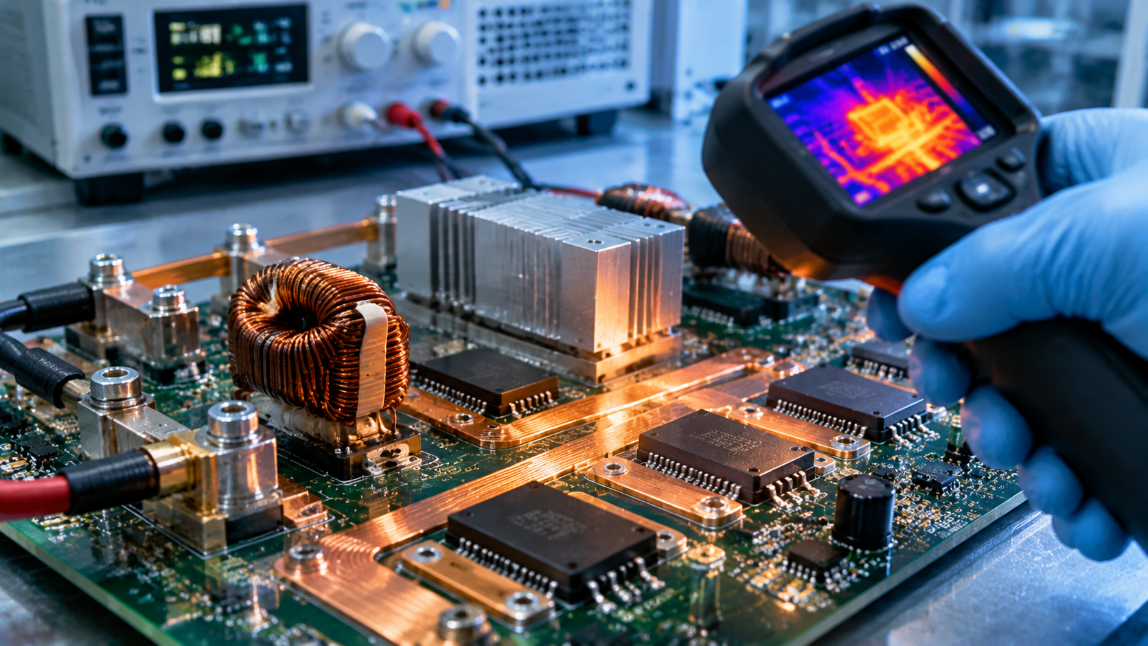
Infrared thermal camera: During prototype testing, use a thermal camera to detect temperature anomalies on the board and identify potential issues early.
High current inevitably brings high heat. Physical thermal measures must be implemented:
Add heatsinks or dense thermal via arrays to the PCB to conduct heat to the backside or inner layers.
For extremely high-load circuits, add external heatsinks or fans beside the PCB components, or even use liquid cooling.
Component selection must account for current and voltage requirements with sufficient margin.
Pay special attention to power inductors, high-current connectors, and MOSFETs. Their rated current and temperature limits must be observed to avoid long-term operation at or near full load, which shortens lifespan or causes burnout.
Safety is paramount in high-voltage, high-current environments:
Ensure sufficient creepage distance and electrical clearance.
Use substrates with excellent insulation (such as high-Tg materials) to prevent arcing and dielectric breakdown.
Isolate high-current areas to ensure overall system safety.
In applications with extremely high reliability requirements (such as automotive BMS):
Use current sensors and temperature sensors (NTC) to monitor operating status in real time.
With MCU firmware, execute derating or disconnect protection immediately when current or temperature anomalies are detected.
Calculating the perfect trace width in simulation is easy. But perfecting heavy copper fabrication in the factory is the real challenge.
At AnyPCBA, for high-current hardware projects, our DFM engineering team helps customers avoid these manufacturing risks:
Heavy copper etching tolerance control: Heavy copper suffers severe undercut during etching. If design trace width is too close to factory capability, the finished trace may be thinner than intended, failing current-carrying requirements.
Large copper pour lamination warpage: Localized heavy copper causes uneven heat distribution during lamination, leading to warpage. We optimize stack-up and symmetrical design to ensure flatness.
Thermal via barrel quality: Via barrel plating must be thick enough to prevent barrel cracks under high-current surges.
Solder void on thermal pads: Large power device thermal pads easily develop voids during SMT. We minimize void rates by optimizing stencil apertures and reflow profiles.
If you're developing high-current hardware—electric vehicle systems, solar inverters, high-power supplies, or AI computing—contact us through our website. AnyPCBA's engineers can provide professional current-carrying assessment and DFM advice at the design stage, ensuring your product is not only excellent on paper but safe and reliable in the physical world.