Introduction: Crosstalk is one of the most common causes of signal distortion and system failure in high-speed PCB designs. It occurs when electromagnetic fields from one trace couple onto an adjacent trace. This guide covers the physical causes of crosstalk—capacitive and inductive coupling—and provides practical strategies for layout, routing, noise suppression, simulation, and manufacturing control to minimize it.
Description: Based on AnyPCBA's small-to-medium volume PCB and PCBA manufacturing experience, this guide explains how to prevent crosstalk in PCB design—covering layout isolation, ground plane continuity, 3W spacing rules, noise suppression, simulation, and manufacturing controls like impedance and back drilling.
In high-speed and high-frequency circuit design, crosstalk is a common culprit behind signal distortion, increased bit error rates, and even system crashes. Crosstalk occurs when the current or electromagnetic field of one signal circuit (the aggressor) couples unwanted noise onto an adjacent circuit (the victim).
As chip pin pitches shrink and signal speeds move toward 112G/224G, crosstalk has become an invisible bottleneck limiting hardware performance.
This article explores the physical causes of crosstalk and provides comprehensive strategies—from layout and routing to manufacturing processes.
Crosstalk fundamentally consists of two coupling mechanisms:
Capacitive coupling (electric field): High-frequency voltage changes inject noise into adjacent lines through parasitic capacitance due to insufficient spacing.
Inductive coupling (magnetic field): Rapid current changes (di/dt) induce noise voltage in adjacent lines through mutual inductance.
Common causes include electromagnetic radiation, signal reflection, excessive routing density, and mismatched interconnect lengths.
During layout, physically isolate "high-risk" and "sensitive" areas. Switching power supplies, relays, and motor drives (strong noise sources) should be kept far from high-precision ADC sampling and low-level signal amplification circuits.
Crosstalk suppression relies heavily on the ground plane. Ground continuity and low impedance must be maintained. Increasing the ground plane area—or adding a complete ground layer between signal layers—dramatically reduces ground loop self-inductance and resistance, lowering noise.
Analog and digital signals must be strictly separated during layout. If analog and digital traces must cross, ensure they are on different layers and isolate the crossing area with a ground plane.
Place different signal types on different layers. For example, route sensitive analog signals on inner layers near ground planes, and digital signals on outer layers (or the opposite side). A well-planned stack-up (such as Signal-GND-Signal-VCC) greatly reduces electromagnetic coupling between traces.
Plan trace direction to avoid long parallel runs and crossings. If parallel routing is unavoidable, add a guard trace (ground trace) between them or increase spacing. For critical clocks, buses, and RF traces, comply with the 3W rule (spacing at least 3× the trace width).
When high-speed traces change layers, vias introduce parasitic inductance. If layer-change vias for adjacent high-speed traces are too close, crosstalk occurs. Increase via spacing and add return ground vias near each signal via.
Power lines are common interference sources. Keep them isolated from sensitive signal lines and away from high-speed traces. For high-current power, use large copper pours rather than thin, long traces.
Appropriate filters suppress noise. For example, use bypass capacitors on power lines and termination resistors or capacitors on high-speed signal lines—absorbing reflections and reducing crosstalk.
Place ground pours on both sides of or around sensitive traces and densely stitch ground vias on the copper. This forms an effective shield, reducing radiation and induction.
Follow electromagnetic compatibility (EMC) principles when designing signal circuits—including proper component selection, smart layout, controlled return paths, and tight coupling of differential pairs.
Before prototyping, use SI (signal integrity) simulation software (such as HyperLynx or ADS) to simulate electromagnetic field distribution. Identify crosstalk risk areas in advance and adjust trace width and spacing.
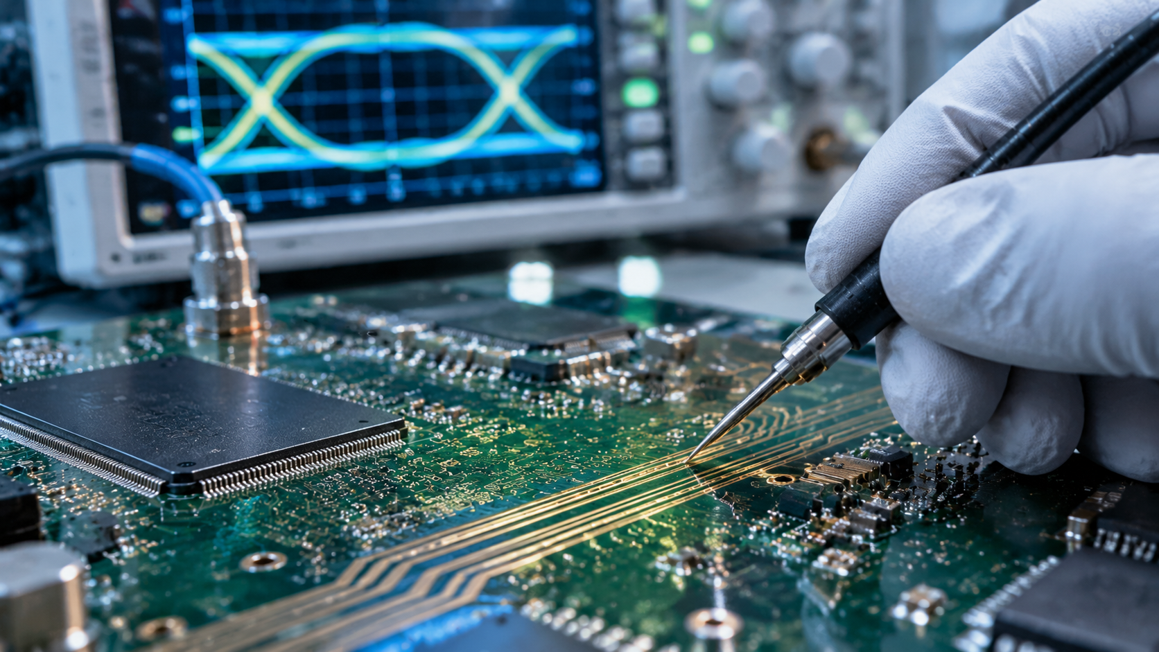
After fabrication, perform engineering validation. Use a TDR (Time Domain Reflectometer) and network analyzer to measure eye diagrams. If crosstalk issues appear in the field, investigate trace spacing, check grounding, and shorten parallel routing to eliminate or reduce crosstalk.
In software, crosstalk can be adjusted through algorithms. In the physical world, crosstalk depends on trace spacing of a few millimeters and dielectric thickness of a few microns.
As a factory focused on small-to-medium volume PCB and PCBA manufacturing, AnyPCBA reduces crosstalk risk through strict process controls:
Precise impedance control: by controlling trace width, spacing, and dielectric thickness, ensuring characteristic impedance is on target and reducing reflections.
High-quality ground planes: during lamination, strictly controlling prepreg resin flow to ensure ground planes are continuous with no voids.
Non-destructive via processes: precise back drilling to eliminate via stubs, reducing crosstalk and reflection caused by vias.
If you're working on high-speed digital, RF, or mixed-signal hardware design and need a manufacturing partner who understands signal integrity and can precisely control impedance, contact us through the AnyPCBA website.