Introduction: Multilayer PCBs stack alternating layers of copper and insulating material, using vias to connect them in three dimensions. This guide covers the basic structure of multilayer boards, four methods to increase routing density—adding layers, optimizing via design, using finer traces, and adopting high-density packaging—and the core advantages they deliver in size, speed, performance, and cost.
Description: Based on AnyPCBA's small-to-medium volume PCB and PCBA manufacturing experience, this guide explains multilayer PCB structure and how routing density is increased—through layer count, via design, fine traces, and high-density packaging—along with the manufacturing constraints that matter.
In electronics engineering, the PCB (Printed Circuit Board) is an essential part of any electronic device. As products become smaller and more highly integrated, multilayer PCBs have gained widespread attention for their higher routing density and superior performance.
This article explains the basic structure of multilayer PCBs, the methods used to increase routing density, and the core advantages this density delivers.
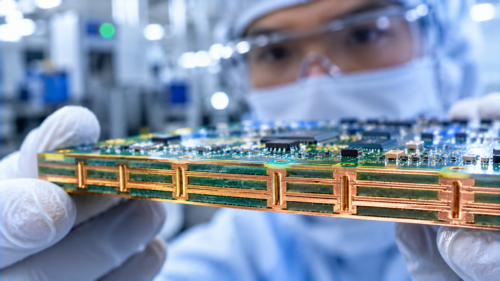
A multilayer PCB is constructed by stacking alternating layers of conductive material (typically copper foil) and insulating material (such as FR-4).
By drilling through these layers and filling the holes with conductive material, conductive paths are formed to connect different layers—these are the vias. This design allows circuits to be routed in three dimensions, greatly increasing routing density.
Multilayer boards are typically laminated from cores and prepregs, with solder mask and silkscreen applied to the outer surfaces.
One significant advantage of multilayer PCBs is the ability to add layers as needed. More layers allow more circuitry to be placed within a limited board area. For example, upgrading from 4 to 6 or 8 layers allows dedicated power and ground planes, freeing up more signal layers.
Vias are the key elements connecting different layers. Optimizing via design—smaller via diameters, more vias, and via filling technologies (resin plugging, via-in-pad)—increases routing density and improves electrical performance.
Multilayer PCB manufacturing precision allows finer traces. Reducing trace width (e.g., from 6 mil to 4 mil or less) allows more circuitry in the same space.
Adopting high-density packaging technologies such as BGA (Ball Grid Array), CSP (Chip Scale Package), and advanced SiP (System in Package) enables higher component density on multilayer boards, further increasing routing density.
Higher routing density enables the same circuit functionality in a smaller footprint, supporting the miniaturization of devices such as smartphones and wearables.
Multilayer designs shorten and simplify signal paths, improving transmission efficiency. Routing high-speed signals on inner layers (stripline) also reduces external interference.
Multilayer PCBs deliver better electrical performance (lower impedance, more complete reference planes) and thermal performance (inner copper layers as heat-spreading planes), improving overall device performance.
Although multilayer PCBs cost more per unit, higher routing density reduces board area and peripheral components, lowering the overall design and manufacturing cost of the device.
At AnyPCBA, we handle everything from simple double-sided boards to high-density 64-layer boards every day.
Multilayer design looks like "just adding copper layers," but on the manufacturing side, each additional layer multiplies process complexity:
Layer registration precision: Higher layer counts demand more precise lamination equipment. Even slight misalignment can cause vias to miss their pads.
Warpage control: Asymmetrical stack-ups or uneven copper distribution cause warpage after lamination, affecting subsequent SMT soldering.
Impedance control: For high-frequency signals, small variations in trace width and dielectric thickness cause impedance mismatch.
Our manufacturing capabilities cover 2 to 64 layers, including HDI, rigid-flex, and high-frequency hybrid. During DFM review, we help customers confirm stack-up symmetry, via processes, and impedance targets—avoiding design failures caused by physical manufacturing limits.
If you're designing high-density multilayer boards, or have questions about manufacturing processes, contact us through the AnyPCBA website.