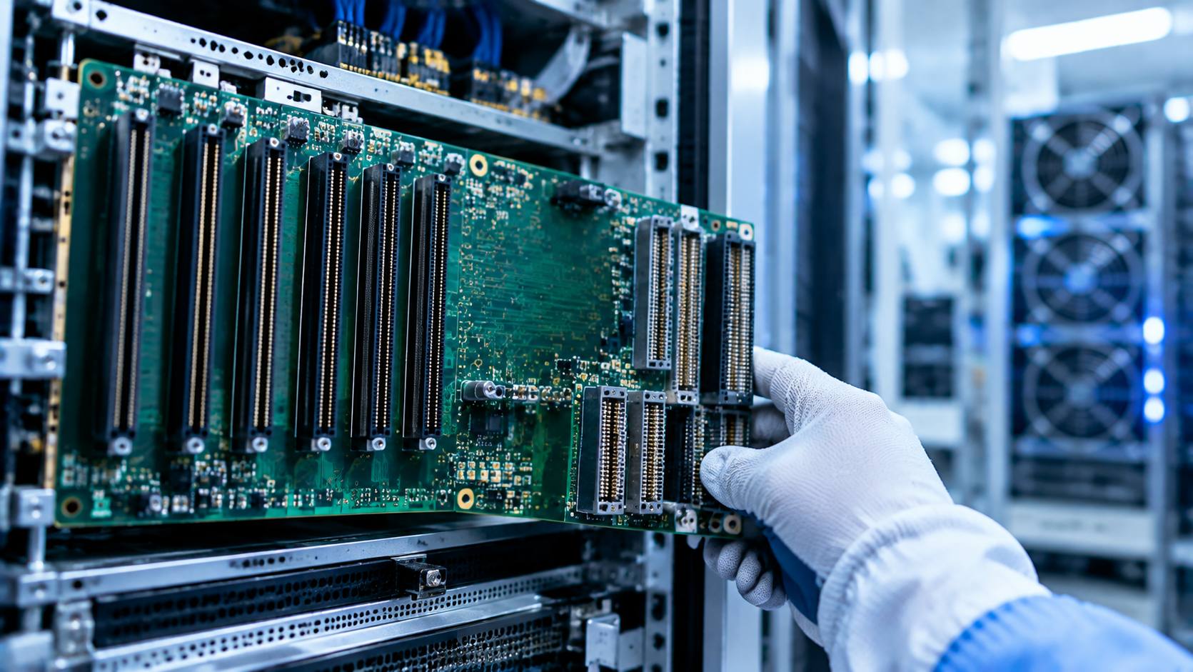
Introduction: A backplane PCB sits at the back or bottom of electronic equipment, supporting and connecting multiple components and subsystems. Unlike standard PCBs, backplanes handle higher layer counts, more connectors, and demanding requirements for signal integrity, power distribution, thermal management, and EMI/EMC. This guide covers their functions, advantages, and manufacturing priorities.
Description: Based on AnyPCBA's small-to-medium volume PCB and PCBA manufacturing experience, this guide explains backplane PCB functions, advantages, and manufacturing priorities—from material selection and layer alignment to thermal management and process control—and how DFM review catches backplane-specific risks before production.
A backplane PCB is a special type of circuit board, typically located at the back or bottom of electronic equipment, used to support and connect various electronic components and subsystems.
Unlike standard PCBs, backplane PCBs have higher layer counts and complexity to accommodate large numbers of connectors, slots, and other connection devices. They also offer higher durability and stability to meet the demanding environments of electronic equipment.
Backplane PCB design typically considers high-speed signal transmission, power distribution, thermal management, and EMI/EMC to ensure equipment stability and reliability. They can be single-layer, double-layer, or multilayer, depending on the equipment's requirements and complexity.
As the stable foundation of electronic equipment, the backplane PCB provides mechanical support and fixation, ensuring the stability and safety of internal components.
Complex circuit networks on the backplane PCB connect various electronic components, chips, modules, and other devices, enabling electrical connection and communication between different parts of the equipment.
The backplane PCB is responsible for transmitting high-speed signals and data, ensuring fast, stable communication between components and the normal operation of the entire electronic device.
The backplane PCB handles power distribution and management, ensuring each component receives stable, reliable power to meet the equipment's power consumption requirements.
The backplane PCB also handles heat conduction and dissipation, helping effectively dissipate internal heat and preventing overheating damage to electronic components.
Backplane PCB design considers electromagnetic interference (EMI) and electromagnetic compatibility (EMC), adopting measures to reduce interference with the external environment and ensure equipment stability and reliability.
Backplane PCBs play a critical role in connection, support, transmission, and management within electronic equipment, directly affecting performance, stability, and reliability.
Backplane PCB design considers maintenance and repair convenience, using modular design and standard interfaces for easy replacement and repair. For example, industrial control system backplanes use modular design so faulty modules can be quickly replaced, reducing repair time and cost.
High-quality materials and advanced manufacturing techniques ensure backplane PCB stability and reliability, maintaining good working condition in various harsh environments. For example, military equipment backplanes use high-reliability materials and processes, verified through strict testing to ensure stability and reliability in battlefield conditions.
Backplane PCB design considers assembly and modularity requirements, allowing flexible combination and assembly with other components to meet different equipment design requirements. For example, industrial automation equipment backplanes can flexibly combine with various sensors, actuators, and other components to achieve complex control functions.
Backplane PCBs offer excellent high-density routing capability, enabling large amounts of signal transmission and processing within limited space, meeting modern electronic equipment's high requirements for data transmission speed and processing capability. For example, server backplanes use high-density routing design to achieve high-speed transmission and processing of large data volumes.
Backplane PCBs can integrate multiple functions and communication interfaces, meeting different equipment function requirements. For example, industrial control system backplanes integrate multiple communication interfaces and control functions, enabling complex control and monitoring functions.
Backplane PCBs are typically thicker and heavier than standard PCBs, so material selection and thickness control requirements are stricter. Choosing appropriate substrates and copper-clad materials—such as FR-4, FR-5, and high-Tg laminates—and strictly controlling board thickness helps ensure mechanical strength, thermal stability, and electrical performance. Material CTE matching must also be considered to avoid deformation or stress concentration when temperature changes, which can affect circuit stability and reliability.
Because backplane PCBs have more layers and more drilled holes, layer alignment becomes a key manufacturing technology. High-precision lamination techniques and advanced alignment equipment ensure layer alignment precision and stability.
Backplane PCB manufacturing requires special process handling, including chemical copper plating, surface treatment, lamination, drilling, and electroplating. These processes require strict control to ensure backplane quality and stability.
Because backplane PCBs are thicker and heavier, heat dissipation and management require special attention during manufacturing. Using heatsinks, heat sinks, fan cooling, and heat pipes, and choosing appropriate thermal materials—such as copper, aluminum, and thermal adhesive—improves backplane PCB heat dissipation efficiency. Thermal simulation and testing evaluate the design's effectiveness, ensuring backplane PCB stability and reliability.
Backplane PCB manufacturing requires strict process monitoring and quality control, ensuring every process and every step meets design requirements and standards. Through detailed manufacturing process specifications, regular equipment maintenance and calibration, strict process parameter control, real-time monitoring and adjustment, and strict inspection and testing of raw materials, processes, and finished products, backplane PCB manufacturing can be stable and reliable, with product quality meeting design requirements and standards.
As a factory focused on small-to-medium volume PCB and PCBA manufacturing, AnyPCBA has accumulated years of experience in backplane PCB manufacturing.
Our manufacturing capabilities cover 2 to 64 layers, including HDI, rigid-flex, and high-frequency hybrid. We hold ISO 13485 (medical) and IATF 16949 (automotive) certifications.
For backplane PCBs, our DFM review and production control focus on:
Material selection and thickness control: choosing appropriate Tg and CTE substrates based on layer count and application, confirming board thickness tolerance and mechanical strength
Layer alignment precision: confirming whether lamination processes can meet alignment requirements for high-layer-count backplanes
Special process feasibility: confirming whether chemical copper plating, lamination, drilling, and electroplating are within factory capability
Thermal management design: confirming whether heatsinks, heat pipes, and other thermal solutions are manufacturable, and whether thermal simulation verification is needed
Warpage control for large backplanes: confirming whether lamination parameters and cooling rates can meet warpage requirements
Connector and slot press-fit processes: confirming whether press-fit hole diameter tolerance and hole wall quality meet requirements
Test coverage: confirming whether high-speed signals and power nets on the backplane have sufficient test points
Our engineers help you confirm these critical details at the design stage, so your backplane is not only drawable, but stable and reliable to produce.
If you're working on backplane PCB design, or want to learn more about our manufacturing capabilities, contact us through our website.




