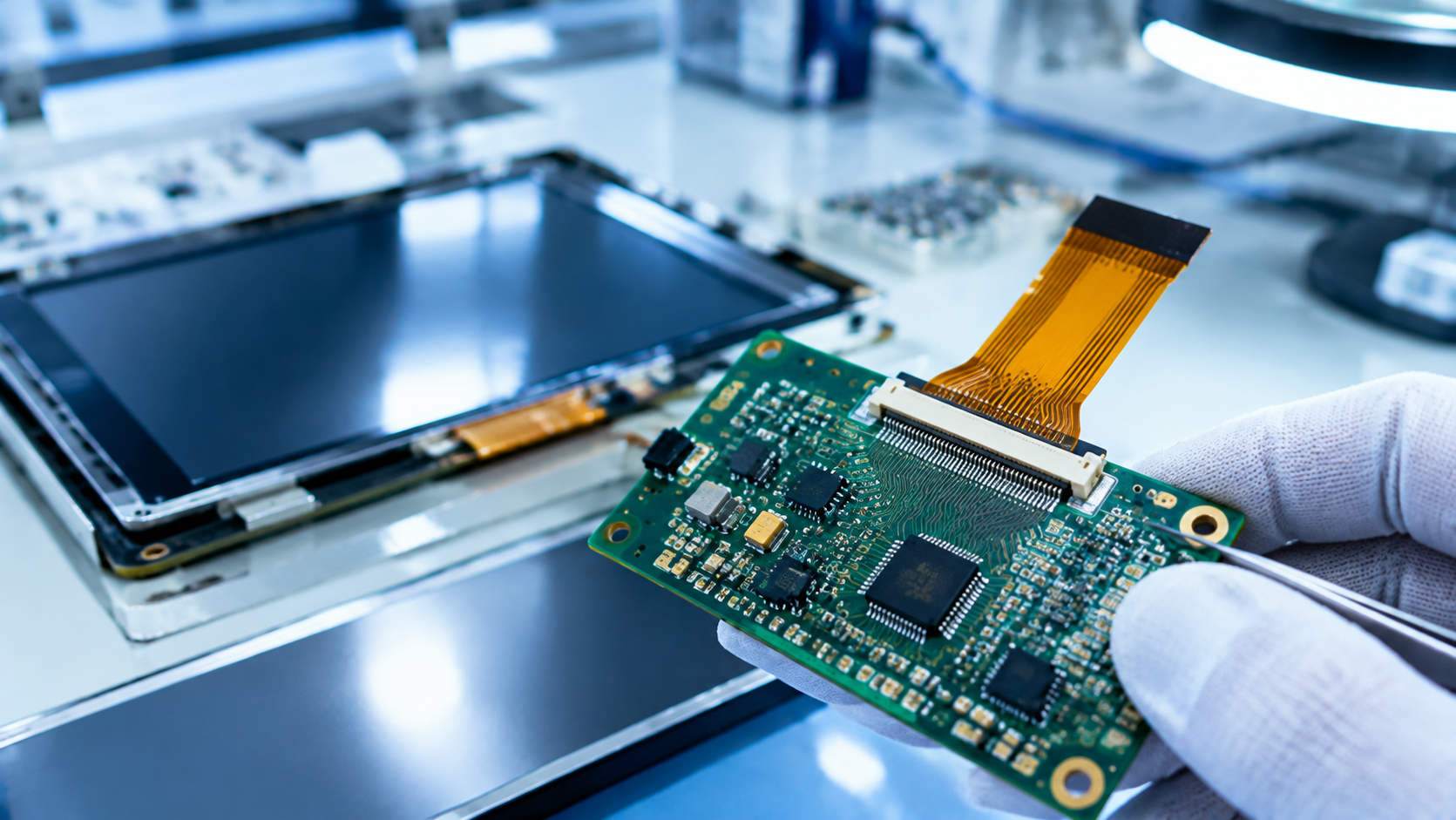
Introduction: LCD and touchscreen technology is at the core of devices from smartphones to medical equipment. PCB design directly affects their performance and reliability. This guide covers signal integrity, power management, interface design (MIPI DSI, LVDS), grounding and shielding, stack-up, layout, thermal management, and serviceability.
Description: Based on AnyPCBA's small-to-medium volume PCB and PCBA manufacturing experience, this guide explains LCD and touchscreen PCB design requirements—from signal integrity and interface design to layout, thermal management, and manufacturability—and how DFM review catches display-related risks before production.
LCD and touchscreen technology has become a core part of electronic devices, from smartphones to televisions and medical equipment. In these devices, PCB design is critical to the performance and reliability of LCDs and touchscreens.
This article covers LCD and touchscreen PCB design requirements from working principles to manufacturability, with AnyPCBA's manufacturing perspective.
Before starting PCB design, it's essential to understand how LCDs and touchscreens work. LCDs use liquid crystals to control light transmission, while touchscreens detect and respond to user touch input. These basic principles are critical to correct PCB design.
Ensure the circuit layout on the PCB considers signal integrity to reduce crosstalk and signal interference. Isolate LCD and touchscreen circuits from other electronic components, and use appropriate ground and power planes for stable electrical performance.
Providing stable power to LCDs and touchscreens is critical. Use appropriate power management circuits to ensure current and voltage stability, preventing display flicker or malfunction.
Design appropriate interface circuits to connect LCDs and touchscreens to the main controller. Considering data transmission rate and signal integrity, choose the correct interface standard, such as MIPI DSI or LVDS.
Proper ground management is key to low noise and high performance. Use appropriate ground layout and shielding techniques to reduce interference and improve signal quality.
When designing the PCB, consider using a multilayer board. This helps isolate different signal layers, reduce crosstalk, improve signal integrity, and provide better thermal performance.
In actual layout, the following points are most often overlooked by engineers—yet they have the biggest impact on manufacturability:
1. Place display interfaces near the board edge.
All display interfaces (whether connectors or FPC) should be placed near the board edge for easy insertion and removal. This affects not only assembly efficiency but also rework accessibility.
2. Keep the main chip and display interface close.
Minimize routing distance. Overly long traces introduce extra parasitic inductance and capacitance, affecting signal integrity.
3. Do not remove decoupling capacitors for the display and touchscreen—place them close to the pins.
Decoupling capacitor placement matters more than capacitance value. Placing them close to the pins effectively suppresses high-frequency noise.
4. Place the LED backlight IC's FB current-limiting resistor near the display connector, not the DC-DC.
This is an easily overlooked detail. The position of the FB current-limiting resistor directly affects backlight current stability.
5. For the backlight boost circuit, pay attention to capacitor placement and power routing.
Minimize the power charge/discharge loop. The smaller the loop area, the lower the EMI and the better the power stability.
6. If test points are reserved on the display and touchscreen connector, place them close to the connector, and keep trace stubs as short as possible.
Excessively long stubs introduce signal reflection and affect high-speed signal quality.
LCDs and touchscreens can generate significant heat. Ensure thermal measures are considered in PCB design, such as heatsinks or thermal pads, to prevent overheating and maintain stable operating temperature.
Considering serviceability, PCB design should ensure easy access to and replacement of LCDs and touchscreens. This is critical to both product lifespan and maintenance cost.
As a factory focused on small-to-medium volume PCB and PCBA manufacturing, AnyPCBA has accumulated years of experience in PCBs for LCD and touchscreen applications.
Our manufacturing capabilities cover 2 to 64 layers, including HDI, rigid-flex, and high-frequency hybrid. We hold ISO 13485 (medical) and IATF 16949 (automotive) certifications.
For LCD and touchscreen PCBs, our DFM review focuses on:
Whether FPC connector placement is assembly- and rework-friendly: whether it's near the board edge and has sufficient access space
Impedance control for MIPI DSI or LVDS differential pairs: whether 100Ω differential impedance requirements are met
Whether decoupling capacitors are close to pins: placement matters more than capacitance value
Whether the backlight boost circuit loop area is minimized: affects EMI and power stability
Whether test points are accessible and stubs are controlled: affects signal integrity and test coverage
Whether thermal paths are sufficient: whether thermal pads, thermal vias, or metal-core boards are needed
Our engineers help you confirm these critical details at the design stage, so your display boards are not only drawable, but stable and reliable to produce.
If you're working on LCD or touchscreen PCB design, or want to learn more about our manufacturing capabilities, contact us through our website.




