
In the race toward miniaturization, Any-Layer HDI has become the gold standard for high-performance PCBs. However, bridging the gap between theoretical density and manufacturing yield requires more than standard design tools; it demands a deep understanding of physics and process constraints. This guide explores the critical DFM parameters that transform complex designs into reliable, mass-producible electronic systems.
The Evolution of Any-Layer HDI Architecture
From Sequential Lamination to Any-Layer HDI
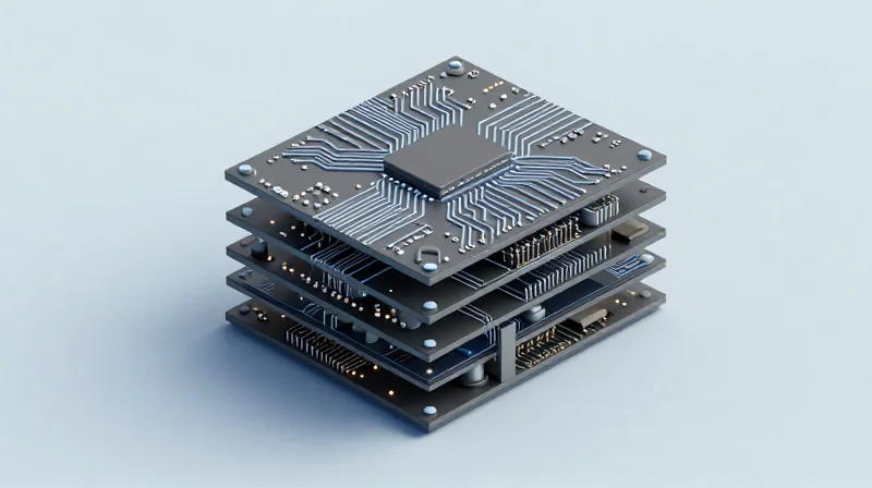
Traditional High-Density Interconnect (HDI) designs relied heavily on sequential lamination, a process where layers are built up in cycles, limiting the ability to route signals freely between any two given layers. Any-Layer HDI, often referred to as 'Every Layer Interconnect' (ELIC), removes these constraints by utilizing laser-drilled microvias that can connect any two adjacent or non-adjacent layers. This breakthrough allows for complete vertical freedom, effectively turning the PCB into a dense, three-dimensional routing matrix.
| Feature | Sequential Lamination | Any-Layer HDI |
|---|---|---|
| Via Structure | Buried and Blind Vias | Stacked Microvias |
| Design Flexibility | Restricted by Lamination Cycles | High - Full Layer Access |
| Component Density | Moderate | Ultra-High |
| Cost Profile | Baseline | Premium |
Key Advantages for High-Density Routing
The adoption of Any-Layer architecture is primarily driven by the need for superior signal integrity and board miniaturization in mobile and automotive applications. By enabling microvias to be stacked anywhere on the board, designers significantly reduce the footprint of via pads, freeing up precious routing channels. This structure minimizes signal stubs and parasitic capacitance, essential for high-speed differential pairs.
- How does Any-Layer HDI improve signal integrity?
By utilizing microvias to create direct paths, you reduce the length of via stubs, which minimizes impedance discontinuities and signal reflections in high-frequency circuits. - What is the primary DFM challenge with Any-Layer HDI?
The main challenge is maintaining alignment accuracy during the laser drilling process across multiple stacked layers, requiring sophisticated registration controls. - Is Any-Layer HDI suitable for all designs?
No; it is typically reserved for space-constrained designs where component density makes standard through-hole or sequential lamination processes physically impossible.
Essential DFM Guidelines for Microvia Design
Critical Aspect Ratios and Laser Drilling Limits
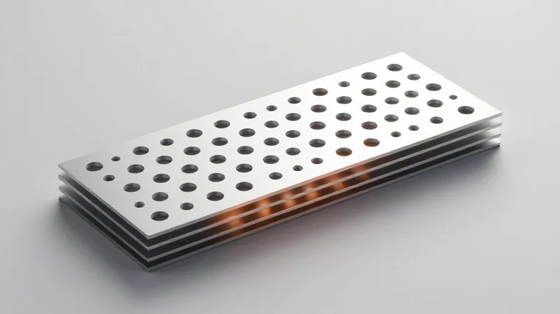
Laser microvias rely on photothermal ablation, which imposes strict geometric limits. To ensure uniform energy distribution and prevent hole-wall roughness or bowing, engineers must adhere to an aspect ratio (depth-to-diameter) typically capped at 1:1 or less. Exceeding this limit often results in poor copper plating coverage, leading to intermittent opens or barrel cracking under thermal stress.
| Feature | Recommended Design Rule | DFM Impact |
|---|---|---|
| Max Aspect Ratio | 1:1 | Prevents plating voids and incomplete laser penetration. |
| Microvia Diameter | 75µm - 100µm | Optimizes laser beam focus and manufacturability. |
| Dielectric Thickness | ≤ 75µm | Ensures clean ablation and effective copper fill. |
Landing Pad Geometry and Capture Requirements
To prevent 'breakout'—where the drill misaligns and cuts into the outer edge of the pad—designers must calculate capture pads based on the fabrication shop's registration capabilities. A safe practice is to design the capture pad at least 75µm larger than the microvia drill size, accounting for layer-to-layer registration tolerances and laser aiming accuracy.
Microvia Design FAQ
- Can I use 'via-in-pad' technology for all microvias?
Yes, but they must be properly planarized and filled with conductive or non-conductive epoxy to prevent voids during subsequent assembly and soldering processes. - How does laser type affect my DFM rules?
CO2 lasers are standard for dielectric removal, while UV lasers are required for drilling through copper-capped vias. If your design mixes materials, verify the stackup limitations with your PCB fabricator. - What is the primary cause of microvia barrel cracking?
Mismatch in Coefficient of Thermal Expansion (CTE) between the copper barrel and the resin dielectric, often exacerbated by a high aspect ratio that prevents optimal plating thickness.
Mastering Laser Microvia Fabrication
Optimizing Laser Drilling Parameters
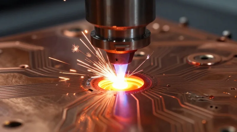
The transition from mechanical drilling to laser ablation is the cornerstone of high-density interconnect (HDI) manufacturing. For any-layer HDI, CO2 and UV lasers are typically used in tandem—UV lasers for copper ablation and CO2 lasers for dielectric material removal. Success in this phase hinges on the calibration of pulse width, frequency, and beam spot size. Achieving a consistent taper angle is critical for effective metallization, as extreme angles can lead to voids in the plating process.
Managing Heat-Affected Zones (HAZ)
Excessive heat during laser ablation causes resin degradation and carbonization, which compromises the integrity of the subsequent electroless copper deposition. To minimize the HAZ, engineers should focus on 'burst mode' drilling techniques and optimized beam expansion. Reducing the thermal impact prevents resin smear, a common failure point that isolates the electrical connection between the via and the target layer.
| Parameter | Control Strategy | Impact on Reliability |
|---|---|---|
| Laser Energy Density | Uniform pulse distribution | Reduces micro-cracking in glass fiber |
| Taper Angle | Beam profile modulation | Improves aspect ratio for plating |
| Resin Smear | Controlled thermal profiling | Ensures reliable inter-layer connection |
The Criticality of Plasma Cleaning
Post-drilling plasma cleaning is not merely a finishing step; it is a chemical requirement to remove debris and de-smear the via barrel. Using an oxygen-CF4 plasma gas mixture effectively etches the exposed dielectric while preparing the copper landing pads for optimal adhesion. Without proper cleaning, the high-density nature of any-layer boards will suffer from intermittent opens or high contact resistance.
Frequently Asked Questions
- How does via aspect ratio affect laser drilling?
A high aspect ratio (typically >0.75:1) increases the difficulty of uniform copper coverage, often necessitating specialized pulse-shaping to ensure the laser does not damage the target pad. - Why is multi-wavelength laser drilling preferred?
Using UV lasers for the copper cap and CO2 lasers for the dielectric allows for 'stop-on-copper' precision, preventing excessive cratering into the landing pad. - What indicates an insufficient plasma cleaning process?
Signs include poor plating adhesion, high via resistance, or 'wedge' voids in the copper barrel during cross-section analysis.
Optimizing Stack-Up Configurations for Reliability
Core Principles of Balanced Stack-Up Design
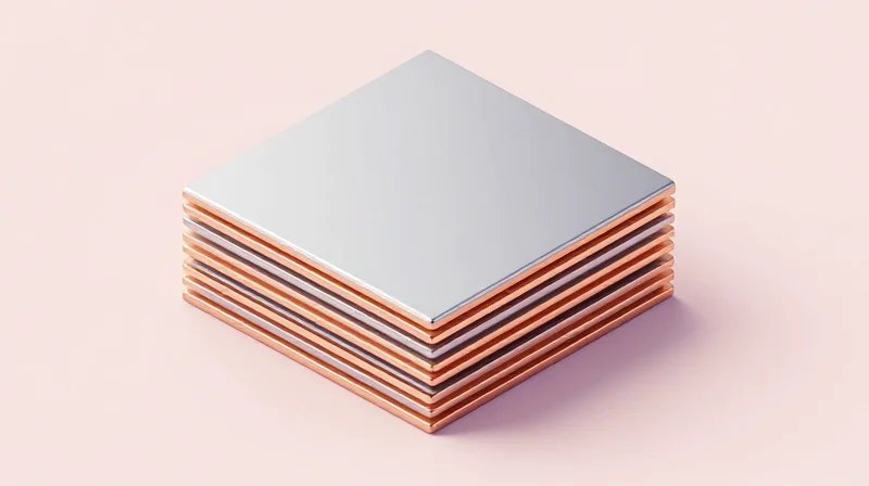
Reliability in any-layer HDI is fundamentally tied to structural symmetry. By ensuring the copper weight and dielectric thickness are mirrored across the board's neutral axis, engineers can prevent warpage during the multiple reflow cycles inherent in high-density builds. Furthermore, selecting high-glass-transition temperature (Tg) materials is essential to withstand the thermal stress of stacked microvia structures.
Thermal Management and Impedance Considerations
| Design Factor | Impact on Reliability | Optimization Strategy |
|---|---|---|
| Copper Distribution | Warpage and Stress | Maintain >80% copper balance per layer |
| Dielectric Choice | CTE Mismatch | Match CTE of laminate to copper |
| Impedance Control | Signal Integrity | Reference every microvia transition |
Frequently Asked Questions on Stack-Up Optimization
- How do you handle impedance discontinuities with stacked vias?
Ensure that the reference planes are consistent across the transition. Avoid referencing floating planes or gaps in the copper pour, as this drastically shifts the characteristic impedance. - Why is material choice critical for any-layer HDI?
Any-layer HDI undergoes significantly more thermal cycles during fabrication. Low-CTE materials reduce the stress on the electroless copper plating inside the laser-drilled microvia barrels. - Is staggered vs. stacked via configuration better for reliability?
Stacked vias save critical routing space, but staggered vias generally offer superior structural integrity by distributing mechanical stress points across different dielectric layers.
Metallization Challenges: Plating Through Microvias
Overcoming Metallization Hurdles in High-Density Interconnects
The primary challenge in plating through-hole and microvia structures lies in achieving uniform copper deposition within high-aspect-ratio (HAR) features. As the ratio of via depth to diameter increases, the mass transport of copper ions into the via becomes restricted. This physical limitation often leads to inadequate plating thickness at the center of the via barrel or, in extreme cases, the formation of voids and barrel cracking due to thermal expansion mismatches between the copper and the dielectric substrate.
Common Plating Defects and Mitigation Strategies
| Defect Type | Primary Cause | Preventative Action |
|---|---|---|
| Barrel Cracking | CTE Mismatch/Stress | Ductile Cu chemistry selection |
| Plating Voids | Air bubbles/Poor wetting | Advanced pulse reverse plating |
| Via Hole Roughness | Incomplete Desmear | Optimized plasma cleaning cycles |
Essential Considerations for Plating Bath Chemistry
To ensure robust interconnects, engineers must prioritize the use of high-throwing-power plating baths. Standard chemistry often fails to adequately penetrate deep microvias, resulting in 'dog-boning'—where the plating is thicker at the surface than in the center. Utilizing pulse reverse plating (PRP) current waveforms allows for more uniform copper distribution by periodically reversing the polarity, which strips excess copper from high-current-density areas and allows ions to deposit more effectively in restricted via geometry.
Frequently Asked Questions: Plating Challenges
- What is the recommended aspect ratio for reliable plating?
While technology varies, a 0.75:1 to 1:1 aspect ratio for laser-drilled microvias is considered optimal for mass-manufacturable plating processes. - How does desmear quality impact plating adhesion?
Incomplete removal of laser ablation debris results in poor copper-to-resin adhesion, which inevitably leads to delamination and interconnect failure during thermal cycling. - Can pulse plating solve all voiding issues?
While pulse plating significantly improves throwing power, it must be paired with precise agitation and surfactant levels in the bath to ensure complete wetting of the via sidewalls.
Thermal Management in Compact HDI Boards
Overcoming Thermal Constraints in HDI
In any-layer HDI (High-Density Interconnect) designs, the drastic reduction in footprint and component density renders traditional bulky thermal solutions obsolete. Heat must be managed at the board level by treating the PCB itself as a primary heat spreader. By leveraging copper microvias and specialized thermal vias as high-conductance conduits, engineers can divert heat from sensitive silicon junctions directly into the internal ground planes, effectively utilizing the PCB's entire cross-sectional area for dissipation.
Key Strategies for Thermal Distribution
- Thermal Microvia Arrays
Implement high-density, copper-filled stacked microvia arrays directly under thermal pads to establish a low-impedance vertical path from top-layer components to inner-layer ground planes. - Integrated Copper Coins
For high-power components where vias are insufficient, embed solid copper coins into the board stack-up during fabrication to provide a direct mechanical and thermal bridge. - Plane Continuity
Ensure internal ground planes remain contiguous beneath high-heat regions. Fragmented planes act as thermal barriers, leading to localized hotspot formation.
Thermal Mitigation Comparison
| Method | Effectiveness | Fabrication Complexity |
|---|---|---|
| Copper-filled microvias | Moderate | Low |
| Embedded copper coins | High | High |
| Expanded ground copper pour | Low | Negligible |
Design for Manufacturing (DFM) Considerations
When incorporating thermal structures, engineers must balance thermal conductivity with structural integrity. Over-populating a region with thermal vias can compromise the board's structural rigidity and interfere with signal trace routing. Always verify with your fabricator that the chosen thermal via pitch allows for adequate copper plating coverage; insufficient plating within the microvia barrel can create high-resistance paths that degrade the intended thermal dissipation efficiency.
Collaboration: Communicating with Your PCB Fabricator
Bridging the Gap: Design Intent vs. Manufacturing Capability
Any-layer HDI (ELIC) technology pushes the limits of modern manufacturing. Because these boards involve complex processes like sequential lamination and laser microvia drilling, treating your fabricator as a design partner rather than a vendor is essential. Engaging early allows you to align your design rules with the fabricator's specific process capabilities, such as their registration tolerances and plating bath chemistries.
Critical Data Points for Fabricator Review
| Data Category | Reason for Review | Risk if Omitted |
|---|---|---|
| Stackup Definitions | Confirms material CTE matching | Delamination during thermal shock |
| Microvia Geometry | Validates aspect ratio vs plating | Voiding and barrel cracking |
| Copper Weight | Aligns with etching capabilities | Impedance deviations |
| Drill Tolerance | Ensures registration accuracy | Open circuits due to misalignment |
Common Collaboration Pitfalls and Solutions
- Why should I share my netlist and impedance requirements early?
Sharing these early allows the fabricator to perform a preliminary DFM check and confirm that your target impedance values are achievable with their current dielectric constants and line width tolerances. - How does stackup planning avoid design delays?
Fabricators often have preferred material sets that are optimized for their sequential lamination process. Using their standard stacks reduces material procurement time and ensures higher process reliability. - Should I provide a custom DFM checklist?
Yes. Providing a project-specific DFM checklist ensures that the fabricator explicitly signs off on your microvia diameters, capture pads, and spacing requirements before you commit to final board layout.
The Impact on Yield and Cost
In any-layer HDI designs, the cost of a failed board is exponentially higher than in standard PCB technology. By implementing a formal 'Design for Manufacturing' review process, engineers can eliminate non-manufacturable geometries before they reach the shop floor. Proactive collaboration converts manufacturing feedback into actionable design constraints, drastically reducing scrap rates and accelerating time-to-market.
Achieving yield success in Any-Layer HDI is a testament to rigorous engineering precision and process control. By adhering to these DFM best practices and fostering close collaboration with your fabrication partner, you can overcome the challenges of extreme density and ensure product longevity. Ready to optimize your next high-performance PCB design? Contact our engineering team today for a comprehensive DFM review of your project files.
