
In the high-stakes world of SMT module design, few features cause as much manufacturing anxiety as castellations. When executed incorrectly, these semi-plated holes can lead to catastrophic short circuits and unreliable solder joints. This manual cuts through the technical noise, providing veteran-level DFM insights to help you perfect your module-to-carrier transitions.
Understanding the Anatomy of a Castellated Hole
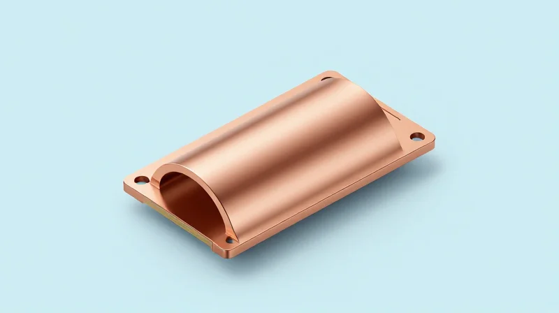
Defining the Castellated Hole
A castellated hole, or 'half-hole,' is a plated through-hole (PTH) that has been bisected during the board edge routing process, leaving a concave, metalized surface on the side of the PCB. This geometry essentially transforms the standard via into a side-mounted pin, allowing a sub-assembly module to be soldered directly onto a primary carrier board as if it were a surface-mount component.
Geometric Anatomy
The structural integrity of a castellated connection relies on the precise alignment of drilling and routing. The anatomy is defined by the remnant copper plating remaining on the concave wall, which serves as the electrical and mechanical contact point. When the router bit cuts through the hole center, it creates the characteristic 'C' shape that provides a high surface area for solder fillets to form between the module and the motherboard.
| Feature | Functional Impact |
|---|---|
| Plated Barrel | Ensures reliable electrical path through the PCB substrate. |
| Router Cut | Determines the finish and cleanliness of the edge contact. |
| Concave Wall | Increases solder wetting surface area for superior joints. |
Common Design Considerations
- Why is drill-to-router registration critical?
Misalignment can lead to partial loss of the copper plating, resulting in weak solder joints and inconsistent electrical impedance. - How does hole size affect manufacturing?
Larger holes provide more surface area but increase the risk of copper burrs during routing; optimal design usually balances hole size with structural rigidity. - Is special surface finish required?
Surface finishes like ENIG or ENEPIG are highly recommended to ensure solderability on the exposed copper edges, preventing oxidation.
Copper-to-Board-Edge Clearance Rules
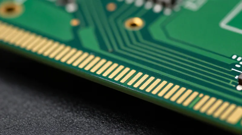
The Critical Importance of Edge Clearance
When castellated holes are drilled through the edge of a PCB, the routing bit acts as a mechanical cutting tool that shears through copper layers. If copper traces or planes are placed too close to the board edge, the physical stress of the routing process can cause copper delamination, tearing, or the creation of 'slivers'—small, conductive burrs that bridge adjacent castellated pads. Maintaining a strict clearance rule is not merely a design preference; it is a fundamental DFM requirement to ensure electrical isolation and mechanical integrity.
Recommended Clearance Guidelines
| Feature Type | Recommended Minimum Clearance | Reasoning |
|---|---|---|
| Copper Traces | 0.30mm (12 mils) | Prevents tearing during mechanical router bit exit. |
| Ground/Power Planes | 0.50mm (20 mils) | Reduces risk of plane delamination and thermal shorts. |
| Non-functional Pads | 0.25mm (10 mils) | Minimizes potential for stray conductive burrs. |
FAQs on Castellated Edge Manufacturing
- Can I place copper right up to the edge for better heat sinking?
No. Copper extending to the edge will inevitably be pulled or smeared by the routing bit, creating conductive debris that can cause shorts during assembly. - Does the board finish type affect clearance requirements?
Yes. Boards using ENIG or HASL may exhibit different levels of edge stress; it is safest to adhere to the strictest clearance guidelines to accommodate the chemical etching and mechanical routing phases. - Why do my pads sometimes look jagged after routing?
Jagged edges are often a symptom of insufficient clearance leading to mechanical tearing. Ensure your design provides a 'pull-back' of internal copper layers to allow for a cleaner cut.
Metalized Hole Plating and Drill Specifications
Drill Specifications and Aspect Ratio
The mechanical drilling of castellated holes involves removing half the barrel, which significantly increases the risk of 'tearing' the remaining copper plating. To mitigate this, standard industry practice dictates a minimum drill diameter of 0.4mm for castellations. Smaller diameters increase the risk of drill wander and structural weakness. Designers must also maintain an aspect ratio of no more than 6:1 relative to the board thickness to ensure consistent plating deposition through the barrel walls.
Plating Integrity and Solder Wetting
Plating thickness is the primary determinant of mechanical and electrical longevity. Insufficient copper density within the half-hole will result in intermittent contact or catastrophic failure during thermal cycling. We recommend a minimum finished copper plating thickness of 25 micrometers (1 mil) inside the hole barrel.
| Feature | Minimum Recommendation | Notes |
|---|---|---|
| Drill Diameter | 0.4 mm | Depends on mechanical stability. |
| Copper Thickness | 25 µm | Essential for structural integrity. |
| Surface Finish | ENIG or ENEPIG | Provides optimal planar wetting. |
Common Manufacturing FAQ
- Why is copper tearing common in castellations?
Tearing occurs when the router bit shears the plated copper barrel during edge profiling. Using a 'pre-drill and plate' approach followed by a clean secondary routing pass with specialized cutting parameters minimizes this. - Does surface finish impact castellation soldering?
Yes. ENIG is preferred because it offers a flat surface for SMT assembly, ensuring that the half-hole retains enough solder to create a robust fillet, whereas HASL can create uneven surfaces that hinder wetting. - What is the role of the plating bath current density?
High-aspect-ratio holes require controlled pulse plating to ensure the metal ions reach the center of the barrel, preventing 'dog-boning' where plating is too thick at the ends and too thin in the center.
Optimizing Pad Design to Prevent Solder Bridging
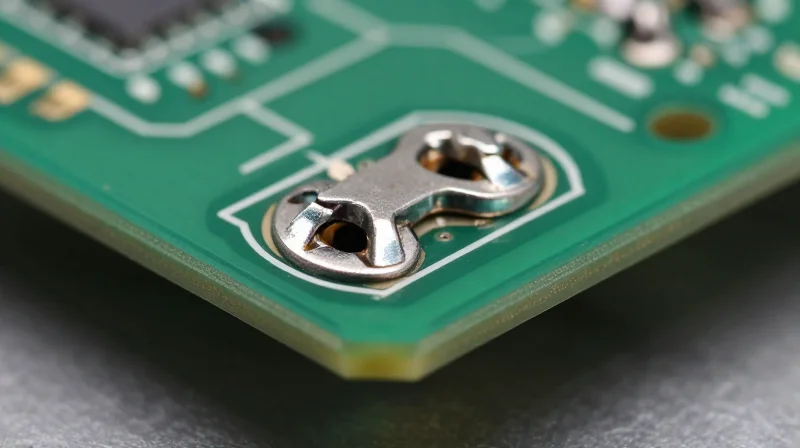
Engineering Pad Geometry to Minimize Solder Bridging
Solder bridging in castellated modules often results from excessive solder paste volume that fails to wet correctly to the side-plated surface. To mitigate this, engineers must adopt a design that restricts paste deposition through optimized aperture ratios and strategic pad extensions. By extending the pad slightly onto the PCB surface—typically 0.25mm to 0.5mm—you create a wetting shelf that pulls solder into the half-hole, reducing the risk of 'solder balling' at the board edge.
Comparison of Pad Design Strategies
| Feature | NSMD (Non-Solder Mask Defined) | SMD (Solder Mask Defined) |
|---|---|---|
| Bridging Risk | Higher due to exposed copper | Lower due to mask constraints |
| Solder Volume Control | Less precise | Highly controlled |
| Recommended Usage | General pads | High-density castellations |
Best Practices for Stencil and Paste Control
The stencil aperture design is as critical as the copper geometry itself. For castellated pads, it is standard practice to reduce the stencil aperture by 10-20% relative to the pad area to prevent excess paste. Additionally, avoid 'full-flood' paste application; use a home-plate or rounded-rectangle aperture shape to direct the solder flow toward the center of the castellation.
FAQ: Solving Common Castellated Solder Issues
- How do I prevent solder wicking along the side of the module?
Implement a solder mask dam between adjacent pads. Even a small 0.1mm strip of mask can significantly break the surface tension path that leads to bridging. - Is there a specific orientation for the stencil?
Yes, orient the aperture apertures to print parallel to the board edge. This ensures that the paste 'bites' into the half-hole during reflow rather than extruding outward. - Why does solder bridging occur specifically at the bottom of the castellation?
This is often due to 'outgassing' or excessive paste volume that pushes solder out of the hole when the component is placed; reducing the pad width at the base of the hole can alleviate this.
Surface Finish Considerations for Castellations
Surface Finish Performance for Castellated Edges
The choice of surface finish for castellated holes directly dictates the ease of assembly and long-term joint integrity. Because castellations involve exposed copper on the vertical cut edge, the finish must protect this surface from oxidation while providing a highly solderable interface that promotes optimal fillet formation.
| Finish | Solderability | Flatness | Suitability for Castellations |
|---|---|---|---|
| ENIG | Excellent | Superior | High (Recommended) |
| HASL | Good | Poor | Low (Risk of Bridging) |
| Immersion Silver | Very Good | Excellent | Moderate (Tarnish Risk) |
Comparative Analysis of Finishes
- ENIG (Electroless Nickel Immersion Gold)
ENIG is the industry standard for castellations due to its excellent planarity. The nickel layer provides a robust barrier, while the gold ensures long-term solderability for the semi-plated holes. - HASL (Hot Air Solder Leveling)
HASL is generally discouraged for fine-pitch castellations. The uneven coating thickness often leads to irregular fillet geometries and increases the risk of solder bridges between adjacent pads. - Immersion Silver (ImAg)
ImAg offers a flat, cost-effective finish that works well for many SMT applications. However, it is susceptible to tarnishing if not handled carefully, and shelf-life limitations must be strictly managed for castellated parts.
Designers should prioritize finish flatness to maintain consistent contact between the module castellations and the motherboard pads. In dense designs, flat surfaces are essential to prevent solder volume variability, which can lead to open joints or unintended shorts across the castellated gap.
Best Practices for Fabrication House Documentation
Communicating Edge-Plating Intent
Clear communication with your PCB manufacturer is the single most effective way to eliminate ambiguities regarding castellated features. Because edge-plating is a non-standard process compared to traditional through-hole drilling, you must provide explicit instructions in your fabrication notes and mechanical drawings to prevent the fabricator from assuming standard tolerances or edge-finishing techniques.
- Why should I specify the exact sequence of drilling and plating?
The sequence of drilling, plating, and routing significantly affects the final quality. Requesting a specific process flow, such as pre-routing or laser-drilling prior to final plate, ensures the fabricator considers the risk of burrs or copper flaking on the castellated edges. - How do I communicate edge-plating boundaries?
Clearly define which portions of the board edge require plating. Do not rely on general notes; instead, use a specific fabrication layer in your Gerber files, clearly labeled, that highlights the exact castellated segments.
Documentation Checklist for Fabricators
| Parameter | Recommended Documentation Requirement |
|---|---|
| Copper Thickness | Specify minimum finished wall copper (typically >25µm) for structural integrity. |
| Edge Integrity | Require a deburring process note to prevent slivers or short circuits. |
| Tolerance | Define specific tolerance for the breakout of the half-hole to maintain pad surface area. |
| Surface Finish | Explicitly require plating continuity for the edge-walls, not just the surface pads. |
Avoiding Common Misinterpretations
Misinterpretations often stem from ambiguous 'Fabrication Notes.' Avoid generic statements like 'Follow IPC-6012.' Instead, supplement IPC standards with explicit, feature-specific requirements. For instance, define the maximum allowable burr size at the edge of the castellated hole, as standard internal hole specifications may be too loose for edge-exposed copper. By providing a detailed 'Edge Plating' detail on your mechanical drill drawing, you transform a potentially problematic design into a standard, reproducible manufacturing process.
Testing and Inspection Strategies for Castellated Joints

Verifying Castellated Joint Integrity
Verification of castellated holes presents unique challenges due to their geometry, which often obscures the internal barrel surface from standard downward-looking automated optical inspection (AOI) systems. To ensure high-reliability interconnections, manufacturers must employ a multi-modal approach combining specialized lighting, cross-sectional analysis, and stringent solder fillet evaluation criteria.
AOI Optimization for Edge-Plated Features
Standard AOI algorithms often fail to detect wetting deficiencies inside the castellation. To overcome this, use multi-angle lighting profiles specifically calibrated for reflective surface curvatures. The goal is to highlight the fillet meniscus against the background of the board edge. If standard AOI is insufficient, move toward 3D SPI (Solder Paste Inspection) or 3D AOI to quantify paste volume before reflow, as solder volume is the primary predictor of successful wetting.
Cross-Section Analysis Criteria
| Inspection Method | Primary Focus | Reliability Insight |
|---|---|---|
| Micro-Sectioning | Intermetallic Compound (IMC) | Detects brittle joint formation or thermal degradation. |
| Dye and Pry | Fracture Path | Determines adhesion strength of the castellation plating. |
| X-Ray (Angled) | Voiding | Identifies internal solder porosity within the hole barrel. |
Common Inspection FAQs
- Why does standard AOI often miss solder voids in castellated holes?
Standard AOI uses vertical lighting which reflects off the curved surface of the castellation, creating glare and shadow that mask the internal joint structure. - What is the acceptable fillet height for a castellation?
Per IPC-A-610 standards, a minimum of 75% coverage of the castellation wall is generally required, though high-reliability designs often mandate 100% wetting for structural integrity. - Is cross-sectioning necessary for every production run?
No, cross-sectioning is a destructive test best reserved for First Article Inspection (FAI) or process qualification to validate the reflow profile and solder paste deposition settings.
Perfecting castellated hole design is an iterative process that rewards precision and strict adherence to DFM standards. By implementing these clearance and plating best practices, you can dramatically improve yield rates and product longevity. Ready to optimize your next PCB design? Contact our engineering team today to review your project files for manufacturing readiness.
