
In the demanding world of industrial lighting, thermal management is not just a feature—it is the lifeline of your product. As power density increases, the margin for error in Aluminum PCB (MCPCB) design vanishes. This guide breaks down the critical DFM engineering principles required to eliminate thermal bottlenecks and ensure your LED drivers operate reliably under extreme stress.
Understanding the Thermal Advantage of Aluminum PCBs
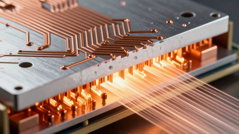
The Thermal Mechanics of Aluminum PCBs
Aluminum PCBs, also known as Metal Core Printed Circuit Boards (MCPCBs), leverage an aluminum base layer to effectively draw heat away from power-intensive LED components. Unlike standard FR-4 substrates that rely on copper planes and thermal vias for heat dispersion, aluminum boards utilize a highly thermally conductive dielectric layer that interfaces directly with the metal base, creating a low-resistance thermal path that significantly enhances component longevity and reliability in harsh industrial environments.
The Role of the Dielectric Layer
The performance of an Aluminum PCB hinges on the quality of its dielectric material. This thin, electrically insulating but thermally conductive layer is the bottleneck for heat transfer. When designing for high-density LED drivers, selecting a dielectric with high thermal conductivity (measured in W/m·K) is critical to prevent localized hotspots that can cause premature diode degradation.
| Substrate Type | Thermal Conductivity (W/m·K) | Primary Thermal Path |
|---|---|---|
| Standard FR-4 | 0.25 - 0.3 | Thermal Vias |
| Aluminum PCB | 1.0 - 5.0+ | Direct Metal Core |
Key Considerations for Industrial LED Applications
- Why is Aluminum preferred for high-density LEDs?
Aluminum allows for higher power density and closer component spacing by mitigating the thermal constraints typically imposed by traditional glass-epoxy substrates. - Does the dielectric thickness impact performance?
Yes; a thinner dielectric layer generally lowers thermal resistance but must be balanced against the required dielectric breakdown voltage to ensure electrical safety. - How does this impact DFM rules?
Designers must account for the mechanical rigidity of the aluminum base, limiting board flexure and ensuring thermal interface materials are applied consistently during assembly.
Calculating Precise Trace Widths for High-Current Flow
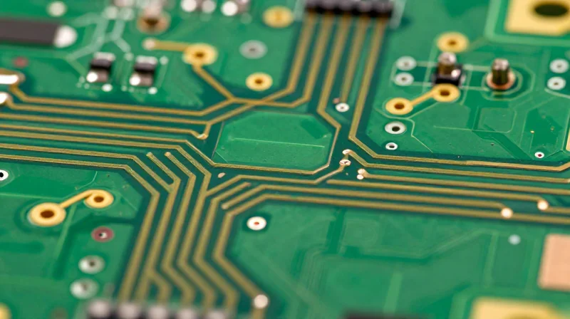
Applying IPC-2152 Standards for Thermal Stability
Unlike outdated legacy IPC-2221 charts, the IPC-2152 standard provides a scientifically rigorous framework that accounts for the specific thermal conductivity of aluminum-backed PCBs. For high-density industrial LED drivers, where currents often exceed 3A, the relationship between conductor width, copper thickness, and allowable temperature rise is non-linear. Designers must prioritize trace geometry to prevent localized hot spots that can degrade the dielectric layer over time.
Determining Current Capacity by Copper Weight
| Copper Weight (oz) | Thickness (mm) | Performance Note |
|---|---|---|
| 1 oz | 0.035 | Standard for low-power signal traces; inadequate for high-current. |
| 2 oz | 0.070 | Common starting point for industrial LED current paths. |
| 3 oz+ | 0.105+ | Recommended for high-density drivers to reduce width requirements. |
Design Best Practices for High-Current Paths
- Should I prefer wider traces or thicker copper?
Thicker copper (e.g., 2 oz or 3 oz) is generally superior for high-current LED drivers because it reduces resistance more effectively than simply increasing trace width, which consumes valuable board space. - How does the aluminum substrate affect calculation?
The metal core acts as an infinite heat sink. When using IPC-2152 calculators, always specify the correct board material to account for the faster heat transfer from the conductor through the thin dielectric into the aluminum plate. - What is the danger of undersizing traces?
Undersized traces cause resistive heating (I²R losses). In an aluminum PCB, excessive heat can cause the prepreg dielectric to delaminate or lose its voltage withstand rating, leading to catastrophic failure.
To ensure reliable performance, use an IPC-2152-compliant calculator to determine the minimum width. Always add a 20% margin to your calculated trace width to account for manufacturing tolerances in copper etching and process variations in high-volume industrial environments.
Managing Dielectric Thickness and Thermal Resistance
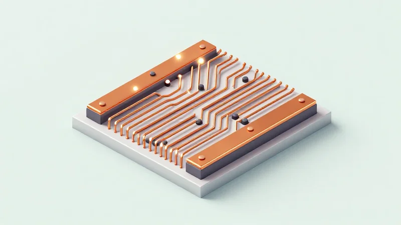
The Thermal-Dielectric Trade-off
The dielectric layer is the primary thermal bottleneck in an aluminum PCB. While a thinner dielectric significantly reduces thermal resistance by shortening the heat path to the aluminum base, it increases the risk of dielectric breakdown under high-voltage industrial conditions. Designers must select a dielectric thickness that maintains sufficient dielectric strength (typically measured in kV) while minimizing thermal resistance to ensure long-term LED reliability.
| Dielectric Thickness (um) | Thermal Resistance | Breakdown Voltage | Typical Application |
|---|---|---|---|
| 50 | Lowest | Low | Low-power high-density designs |
| 75 | Moderate | Standard | General industrial drivers |
| 100+ | Highest | High | High-voltage isolation requirements |
Optimizing Material Performance
Beyond thickness, the thermal conductivity of the dielectric polymer—often filled with ceramic particles—is critical. Standard FR-4 dielectrics are insufficient for industrial LED drivers, as their thermal conductivity is too low (typically 0.2-0.3 W/m·K). High-performance aluminum PCBs utilize specialized thermally conductive prepregs with values ranging from 1.0 to 3.0 W/m·K, effectively bridging the heat gap without requiring excessive dielectric thinning.
Frequently Asked Questions
- How does dielectric thickness impact manufacturing yields?
Extremely thin dielectric layers (below 50um) are more prone to pinholes during lamination, which can lead to shorts between the copper layer and the aluminum substrate, negatively impacting manufacturing yields. - Is thermal conductivity constant across all dielectric types?
No, thermal conductivity is highly dependent on the ceramic filler loading. Higher loading increases thermal conductivity but can make the material more brittle and difficult to process during PCB fabrication. - What should be the priority in high-density drivers?
For high-density drivers, priority should be placed on materials with high thermal conductivity (2.0 W/m·K or higher) to maintain manageable dielectric thicknesses that ensure both robust electrical insulation and efficient heat transfer.
Solder Mask and Surface Finish Limitations
Selecting Thermally Stable Solder Masks
Standard solder masks are often insufficient for high-density LED drivers, which frequently operate at temperatures exceeding 105°C. For aluminum boards, selecting a high-Tg (glass transition temperature) solder mask is mandatory to prevent thermal degradation, peeling, or loss of dielectric integrity during continuous operation. We recommend utilizing thermally conductive solder masks that improve heat dissipation directly from the component pads to the dielectric interface.
Comparison of Common Surface Finishes for Industrial Drivers
| Finish | Thermal Reliability | Best Use Case |
|---|---|---|
| HASL (Lead-Free) | Low | Low-cost, non-critical thermal applications |
| ENIG | Medium | Fine-pitch components, high oxidation resistance |
| Immersion Silver | High | Excellent heat transfer, cost-effective for LED arrays |
| ENEPIG | Very High | Extreme thermal cycling and harsh chemical environments |
Surface Finish and Solder Mask FAQ
- Why is HASL generally discouraged for high-density aluminum boards?
HASL creates uneven surfaces that make placing fine-pitch LED drivers difficult, and the thermal shock during processing can stress the bond between the copper and the dielectric. - How does surface finish affect heat dissipation?
While the finish layer is thin, finishes like ENIG can add a layer of intermetallic resistance; Immersion Silver or ENEPIG are often preferred when maximizing thermal conductivity at the component-to-pad interface. - Can I use standard solder mask colors?
Yes, but be aware that white solder mask—commonly used for light reflection in LED products—can have different thermal expansion coefficients than green. Always verify the CTE (Coefficient of Thermal Expansion) with your fabricator for high-wattage designs.
Effective Stack-up Strategies for Thermal Conductivity
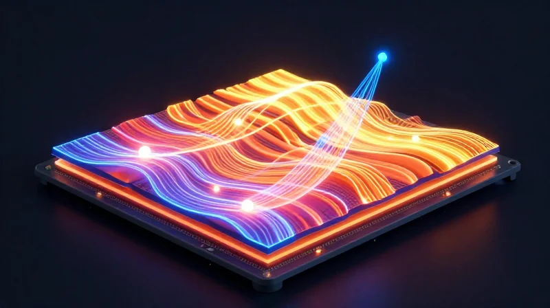
Optimizing Layer Stack-up for Maximum Thermal Conductivity
The primary objective in aluminum PCB stack-up design for industrial LED drivers is to minimize the thermal path length from the junction to the metal base. By prioritizing thin, high-thermal-conductivity dielectric layers and maximizing copper weight in localized regions, designers can significantly lower junction temperatures and extend the lifespan of high-power LED arrays.
Strategic Material Selection and Layer Arrangement
| Material Layer | Thermal Strategy | Design Consideration |
|---|---|---|
| Copper Circuit | Increase thickness for heat spreading | Use 2oz to 3oz copper for high-current paths |
| Dielectric | Minimize thickness while maintaining V-breakdown | Target <75µm for optimal thermal transfer |
| Aluminum Core | Ensure high surface flatness | Utilize 5052 or 6061 alloys for heat sink interface |
Frequently Asked Questions
- How does dielectric thickness affect thermal performance?
Thermal resistance is directly proportional to the thickness of the dielectric. Reducing the dielectric layer thickness provides the most immediate reduction in thermal impedance, provided electrical isolation requirements are met. - Why is copper weight vital in stack-up design?
Heavier copper weight acts as a horizontal heat spreader, effectively increasing the surface area for heat to transfer into the dielectric and subsequently the aluminum core, preventing localized hot spots. - Should I use thermal vias in aluminum PCBs?
In standard single-layer metal-core PCBs (MCPCBs), thermal vias are rarely required because the entire bottom layer serves as a massive heat sink; however, in multi-layer designs, vias are critical to bridge inner-layer heat to the base.
Component Placement and Thermal Spreading Techniques
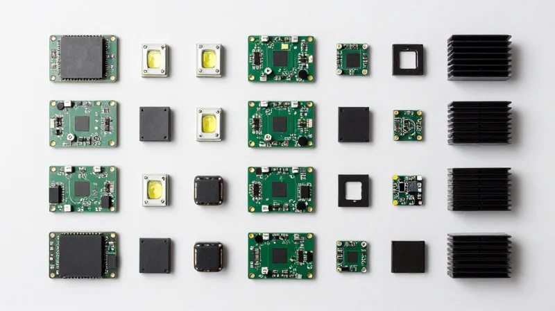
Optimizing thermal performance on aluminum PCBs requires a two-pronged approach: maximizing heat dissipation pathways for power semiconductors and ensuring a uniform temperature distribution across the substrate to prevent localized hotspots that degrade component lifespan.
Strategic High-Power Component Placement
In high-density industrial LED drivers, power components like MOSFETs, Schottky diodes, and inductors should be placed to encourage natural thermal spreading. Avoid grouping multiple heat-generating devices together in a single localized area. Distributing these components across the board allows the aluminum base to utilize its total surface area for passive heat dissipation, effectively lowering the junction temperature of sensitive driver ICs.
Thermal Spreading Techniques and Via Implementation
While aluminum PCBs benefit from the inherent thermal conductivity of the metal core, local heat management remains critical. Integrating thermal vias directly under high-power pads ensures a low-resistance path to the dielectric layer. For optimal results, utilize copper-filled and capped vias to improve conductivity and prevent solder wicking issues during the reflow process.
| Technique | Primary Benefit | Implementation Note |
|---|---|---|
| Distributed Layout | Uniform Heat Spreading | Avoid thermal crowding near ICs |
| Copper-Filled Vias | Reduced Thermal Resistance | Ensure plating thickness > 25um |
| Thermal Landing Pads | Increased Heat Transfer Area | Must be solder-mask defined |
Thermal Management FAQ
- Why is component grouping a DFM risk?
Grouping heat-intensive components creates concentrated heat zones that the dielectric layer cannot effectively dissipate, leading to accelerated aging or thermal runaway of adjacent sensitive silicon. - How do thermal vias function on an aluminum PCB?
Thermal vias act as vertical conduits that bridge the gap between copper traces and the thermally conductive dielectric, allowing heat to flow efficiently into the aluminum substrate. - Is there a limit to thermal via density?
Yes. Excessive via drilling can weaken the structural integrity of the dielectric layer and potentially cause shorting to the aluminum base; always maintain proper clearance and adhere to manufacturer drilling guidelines.
Mitigating Potential Manufacturing Defects
Addressing Dielectric Integrity and Delamination
Delamination remains the most critical defect in aluminum-based PCBs, often stemming from insufficient adhesion between the metal base and the dielectric layer under high-temperature cycling. To mitigate this, designers must specify high-Tg (glass transition temperature) dielectric materials and ensure that the aluminum core is pre-treated to maximize surface energy for optimal bonding.
Common Defect Comparison
| Defect Type | Primary Cause | Mitigation Strategy |
|---|---|---|
| Delamination | Thermal expansion mismatch | Specify high-Tg dielectrics |
| Short Circuits | Burr formation on metal edges | Controlled edge routing/deburring |
| Dielectric Voids | Insufficient lamination pressure | Vacuum-assisted lamination processes |
Managing Short Circuit Risks in Metal-Core Boards
Short circuits frequently occur when conductive particles or metal burrs from the aluminum base migrate into the dielectric layer during drilling or shearing processes. Implementing a 'keep-out' zone at the board perimeter where the copper layer is pulled back significantly from the aluminum edge is essential to preventing creepage paths.
Manufacturing FAQ
- How do I prevent burrs during aluminum substrate cutting?
Utilize precision CNC routing rather than shearing to ensure clean edges, followed by a rigorous deburring station to remove metallic remnants. - Why does thermal cycling cause dielectric cracking?
Cracking typically occurs when the coefficient of thermal expansion (CTE) of the dielectric is not matched closely enough with the aluminum base, leading to stress fractures. - What is the best way to verify bond integrity?
Implement cross-sectional analysis on sample boards from every production batch to inspect for voids or gaps at the metal-to-dielectric interface.
Validation Through Thermal Simulation
The Role of Thermal Simulation in DFM
Thermal simulation acts as a virtual prototyping phase, allowing engineers to visualize heat flux through the dielectric interface into the aluminum base plate. By importing design files into software like Ansys Icepak or Flotherm, designers can verify that the junction temperature of power MOSFETs remains within safe operating limits, preventing premature component failure and ensuring long-term reliability in high-density LED applications.
Simulation Parameters and Best Practices
| Parameter | Importance | DFM Impact |
|---|---|---|
| Dielectric Conductivity | High | Limits heat transfer to base |
| Ambient Temperature | Critical | Defines cooling headroom |
| Airflow Velocity | Moderate | Affects convective efficiency |
Frequently Asked Questions
- Why is steady-state simulation not enough?
Steady-state analysis provides a baseline, but transient simulations are required to identify thermal spikes during rapid LED dimming or power-up cycles that can delaminate dielectric layers. - Does thermal simulation replace prototyping?
No, it reduces the need for multiple physical iterations by weeding out poor layout designs, but final hardware validation via infrared thermography remains essential for golden board certification. - How does aluminum core thickness influence model accuracy?
Modeling the precise thickness of the aluminum base is vital because it acts as the primary heat sink; incorrect values lead to significant inaccuracies in predicting surface isotherms.
Optimizing your Aluminum PCB design is a critical balance of thermal physics and manufacturing precision. By adhering to these DFM best practices, you ensure your industrial LED drivers deliver peak performance and long-term durability. Ready to elevate your hardware reliability? Contact our engineering team today to review your current PCB design for thermal efficiency.
