
In the cutthroat world of satellite communication, a single signal degradation can compromise an entire mission. As data demands skyrocket, designing for high-frequency multilayer PCBs has moved beyond standard practices into the realm of precision engineering. To ensure your satellite transceiver systems perform flawlessly in the vacuum of space, you must align your design intent with strict manufacturing protocols.
Understanding High-Frequency Signal Integrity Challenges

The Physics of High-Frequency Signal Degradation
In satellite communication systems operating at microwave and millimeter-wave frequencies, signal integrity is primarily challenged by the transition of electrical energy from pure conduction to complex electromagnetic wave propagation. As frequencies increase, the signal is no longer confined to the center of the conductor, and the insulating substrate begins to exhibit dissipative properties that can cripple link budgets.
Skin Effect and Surface Roughness
At high frequencies, the skin effect restricts current flow to the outer perimeter of the copper trace. The effective resistance of the conductor increases proportionally with the square root of the frequency. Crucially, copper foil roughness significantly exacerbates this effect; the effective path length for electrons increases as they traverse the microscopic peaks and valleys of the copper surface, leading to substantial insertion loss.
Dielectric Loss and Material Selection
Dielectric loss, defined by the dissipation factor (Df) of the substrate, represents the energy converted into heat as the electromagnetic field polarizes the dielectric material. For satellite applications, selecting materials with a low and stable Df over varying temperatures and humidity is mandatory to maintain signal fidelity.
| Challenge | Primary Physical Cause | Design Impact |
|---|---|---|
| Skin Effect | Frequency-dependent current crowding | Increased ohmic losses and heat |
| Dielectric Loss | Dipole oscillation in substrate | Signal attenuation and dispersion |
| Copper Roughness | Microscopic surface geometry | Added resistance beyond skin effect |
Frequently Asked Questions on Signal Integrity
- How does surface roughness impact high-frequency performance?
Surface roughness increases the effective path length of the signal at high frequencies, resulting in higher insertion loss compared to smooth copper foils. - Why is the Dissipation Factor (Df) critical for satellite boards?
A high Df causes significant energy absorption within the PCB substrate, which directly reduces the power level of the transmitted and received signals, potentially degrading the signal-to-noise ratio.
Advanced Impedance Control Strategies
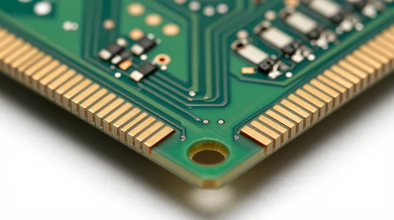
Advanced impedance control in multilayer boards is not merely about initial design calculations; it is about maintaining a consistent transmission line environment across mass production. As frequencies push into the K and Ka bands, the margin for error in trace width and dielectric thickness diminishes, necessitating a holistic approach to manufacturing tolerance management.
Strategies for Dielectric and Copper Consistency
The stability of the Dielectric Constant (Dk) is the primary driver of signal velocity and impedance consistency. For satellite applications, selecting materials with a stable Dk across temperature fluctuations is mandatory. Furthermore, copper foil surface roughness significantly impacts effective impedance at high frequencies due to the skin effect; utilizing low-profile or rolled copper is an essential DFM practice to mitigate insertion loss and phase instability.
| Parameter | Design Strategy | Manufacturing Impact |
|---|---|---|
| Copper Profile | Specify VLP/HVLP copper | Reduces signal skin effect loss |
| Etch Factor | Adjust phototool compensation | Controls final trace trapezoid geometry |
| Dk Tolerance | Use PTFE-based laminates | Ensures velocity consistency |
Frequently Asked Questions on Impedance Control
- How does etch undercut affect high-frequency performance?
Etch undercut creates a non-rectangular trace cross-section, changing the effective width and shifting the calculated impedance. Designers must apply an etch compensation factor to the layout to ensure the final copper width meets target impedance. - Why is copper weight management critical for satellite PCBs?
Excessive copper thickness increases the surface area for dielectric-copper interaction and complicates fine-pitch etching, leading to unpredictable impedance shifts. Standardizing on 0.5 oz or lighter copper is preferred for precision RF routing. - Can solder mask thickness impact impedance?
Yes, the presence of solder mask over RF traces alters the effective dielectric constant of the surrounding medium, typically lowering impedance. Designers should specify 'mask-defined' clearances or 'no-mask' zones for critical high-frequency transmission lines.
Optimizing Layer-to-Layer Registration
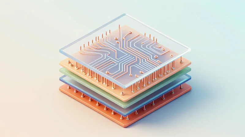
The Imperative of Registration Accuracy
In multilayer high-frequency circuits, registration accuracy dictates the alignment between signal layers and their reference planes. Any deviation—commonly known as registration error or layer misregistration—introduces parasitic inductance and capacitance, causing impedance discontinuities that degrade signal performance in satellite transceivers.
Common Causes of Registration Drift
| Factor | Impact Mechanism | Mitigation Strategy |
|---|---|---|
| Material Thermal Expansion | Differential movement of dielectric layers during lamination. | Select low-CTE glass-reinforced laminates. |
| Tooling Hole Wear | Mechanical tolerances in drilling and pinning systems. | Implement optical registration systems. |
| Circuit Pattern Scaling | Copper density variations causing uneven stress distribution. | Utilize thieving patterns to balance density. |
Technical Best Practices for DFM
- How do copper thieving patterns aid registration?
By distributing copper area evenly across the board surface, thieving minimizes differential etching rates and thermal expansion gradients during the lamination cycle. - Why is the via-to-pad tolerance critical in high-frequency design?
Tight tolerances ensure that via-in-pad transitions remain centered, preventing stub length variations that act as capacitive loads at GHz frequencies. - What is the recommended approach for fiducial placement?
Place global fiducials at the corners of the panel and local fiducials near critical BGA footprints to provide the manufacturing line with precise machine-vision references.
Designers should standardize on non-conductive filler materials for sub-layer bonding and ensure that artwork compensation factors are adjusted based on the specific material's shrink rate data provided by the laminate manufacturer.
Selecting Specialized Surface Finishes for RF Applications
The Impact of Surface Finish on RF Performance
In high-frequency satellite applications, the surface finish is not merely a corrosion barrier; it acts as an extension of the conductor at the surface, directly influencing insertion loss and phase stability. As frequency increases, the skin effect restricts current flow to the outer microns of the trace, meaning that the composition and surface roughness of the metallic plating become dominant factors in signal attenuation.
| Surface Finish | RF Suitability | Primary Advantage | Environmental Robustness |
|---|---|---|---|
| ENIG | Moderate | Excellent Solderability | High |
| ENEPIG | High | Gold Wire Bonding | Superior |
| Immersion Silver | Excellent | Low Signal Loss | Low/Moderate |
Comparative Analysis of Industry Standard Finishes
- Why is ENIG sometimes problematic for RF?
While Electroless Nickel Immersion Gold (ENIG) offers a flat surface, the nickel layer is ferromagnetic, which can introduce skin-effect losses and intermodulation distortion at higher microwave frequencies. - Is Immersion Silver better for high-frequency signal integrity?
Yes, Immersion Silver avoids ferromagnetic materials entirely, resulting in superior performance for high-frequency signal paths; however, it requires strict handling protocols to prevent tarnish and silver migration. - What role does ENEPIG play in complex satellite modules?
Electroless Nickel Electroless Palladium Immersion Gold (ENEPIG) provides the versatility needed for hybrid boards that combine surface mount components with gold-wire bonding, offering a stable barrier that prevents nickel migration into the gold layer.
Designers must balance electrical performance with structural durability. For satellite missions where the board is exposed to vacuum and thermal cycling, the risk of silver oxidation or 'whiskering' must be weighed against the insertion loss benefits. In multi-layer designs, using specialized finishes selectively—applying Immersion Silver to high-speed RF pads and ENIG/ENEPIG to standard components—is a professional DFM strategy to ensure both signal integrity and assembly reliability.
Dielectric Material Selection and Thermal Management
Material Selection Criteria for High-Frequency Space Applications
In satellite applications, dielectric materials must balance low dissipation factors (Df) with exceptional dimensional stability and thermal endurance. PTFE-based laminates remain the gold standard for high-frequency performance due to their low dielectric constant (Dk) stability across broad frequency ranges, though their mechanical softness necessitates specialized handling during fabrication.
| Material Type | Key Advantage | Thermal Limitation | Space Suitability |
|---|---|---|---|
| PTFE Composites | Lowest loss tangent | High CTE (Z-axis) | Excellent (for RF) |
| Hydrocarbon/Ceramic | Dimensional stability | Moderate Df | High (for Digital/RF) |
| Polyimide | Excellent thermal shock | Higher moisture absorption | High (for Flex/Rigid-Flex) |
Thermal Management and Outgassing Considerations
Thermal cycling in low earth orbit requires materials with balanced Coefficient of Thermal Expansion (CTE) to prevent via barrel fatigue and delamination. Furthermore, all materials must pass rigorous NASA ASTM E595 standards for Total Mass Loss (TML) and Collected Volatile Condensable Material (CVCM) to ensure that outgassed chemicals do not degrade sensitive optics or sensors on the satellite bus.
Frequently Asked Questions on Dielectrics
- How does moisture absorption affect high-frequency performance?
Moisture absorption increases the dielectric constant and loss tangent, leading to signal phase shifts and attenuation. Materials for satellite use must feature low hygroscopic properties to maintain stability in a vacuum. - Why is Z-axis CTE critical for multilayer boards?
During thermal cycling, mismatched Z-axis expansion causes stress on plated-through-holes (PTHs). High-frequency materials with high Z-axis CTE require specialized hole-filling resins or reinforced fiber weaves to maintain structural integrity. - Is PTFE inherently difficult to process?
Yes, PTFE exhibits low surface energy and high thermal expansion. Fabrication requires plasma etching for through-hole activation and careful pressure/temperature profiling during lamination to avoid delamination.
Minimizing Via Stub Effects and Signal Reflection
The Impact of Via Stubs on High-Frequency Signal Integrity
In high-frequency multilayer designs, a via stub—the unused portion of a via barrel—acts as an open-ended transmission line. When signal frequencies increase, these stubs resonate at specific wavelengths, causing severe signal notches and reflections that degrade return loss. For satellite transceivers operating in the Ka-band or higher, even a sub-millimeter stub can introduce unacceptable insertion loss.
Mitigation Strategies: Back-Drilling vs. Blind Vias
| Method | Mechanism | Primary Advantage | Manufacturing Cost |
|---|---|---|---|
| Back-Drilling | Secondary drilling to remove stub | Reduces resonance in thick boards | Moderate |
| Blind Vias | Laser ablation of specific layers | Eliminates stubs by design | High |
| Microvias | High-aspect-ratio laser drilling | Minimal footprint | Very High |
Critical DFM Rules for Stub Management
- How is back-drilling tolerance calculated?
The depth tolerance of back-drilling should be strictly controlled within +/- 50 to 100 microns, ensuring that the remaining stub is shorter than 0.25mm to avoid resonance near the operational frequency. - What is the rule for via pad and antipad clearance?
Increase antipad sizes in signal transition planes to reduce parasitic capacitance, which directly minimizes impedance discontinuities when signals move between layers. - How do we handle via-to-trace transitions?
Always employ ground stitching vias around signal vias to maintain continuous return current paths, effectively reducing the loop area and minimizing electromagnetic radiation.
For designs exceeding 20GHz, designers should prioritize the use of microvias and blind vias over traditional through-hole configurations. While back-drilling is a reliable mechanical solution for boards with high layer counts, it requires precise registration to ensure the drill bit does not clip the signal layer, which would render the board non-functional. Adhering to these DFM constraints ensures consistent electrical performance in harsh space-grade environments.
Collaboration Protocols with PCB Fabricators
Establishing a Collaborative Foundation
Bridging the gap between design engineering and fabrication requires proactive communication regarding layer stack-up tolerances, impedance control, and material constraints. By engaging with your fabricator's engineering team during the pre-layout phase, you can align your design choices with their specific equipment capabilities, effectively preventing costly production delays and cycle-time bottlenecks.
Data Exchange Formats Comparison
| Format | Advantage for RF Design | Limitations |
|---|---|---|
| Gerber X2 | Includes stack-up and impedance data | Fragmented data structure |
| ODB++ | Comprehensive intelligent dataset | Proprietary format dependence |
| IPC-2581 | Unified vendor-neutral standard | Adoption rates vary by fabricator |
Key Protocols for Successful Handoff
- How do I ensure impedance consistency?
Provide a detailed stack-up drawing that specifies dielectric constants and tolerances for each high-frequency layer, and request the fabricator's TDR test report. - What should be included in the fabrication notes?
Clearly define controlled impedance requirements, hole size tolerances, and specific surface finish specifications to avoid manufacturing ambiguity. - How can I prevent panelization issues?
Share your board outline early to allow the fabricator to optimize array layout, minimizing waste of expensive PTFE-based laminate materials.
Ultimately, a 'design-for-manufacturing' mindset must extend beyond the CAD workstation. Conducting a Design Review with your PCB supplier before finalizing the release package allows them to flag potential issues—such as non-standard drill aspect ratios or plating thickness variances—that could compromise the integrity of high-frequency satellite communications.
Rigorous Testing and Quality Assurance Standards
Validation of Signal Integrity and Impedance Control
At high frequencies, even minor deviations in trace geometry or dielectric constant result in signal degradation. Time Domain Reflectometry (TDR) serves as the primary diagnostic tool for validating characteristic impedance across multilayer stacks. By launching high-speed pulses into the transmission lines, engineers can pinpoint discontinuities caused by via transitions or laminate inconsistencies. Standard practice requires TDR measurements on both production panels and dedicated test coupons to verify that fabricated impedance remains within the design-specified +/- 5% tolerance.
Structural Integrity via Micro-sectioning
Micro-sectioning provides the microscopic proof required to validate the structural reliability of vertical interconnects and multilayer lamination. By cross-sectioning critical areas of the PCB, inspectors evaluate barrel plating thickness, hole wall quality, and the absence of inner-layer separation or 'measling.' This destructive testing method is vital for detecting subtle voids in the plating that could lead to catastrophic interconnect failure under the extreme mechanical stresses of a launch.
Comparative Overview of Space-Grade Testing Methods
| Testing Method | Primary Metric | Reliability Objective |
|---|---|---|
| TDR Analysis | Impedance (Ohms) | Signal Integrity |
| Micro-sectioning | Plating/Lamination Integrity | Structural Reliability |
| Thermal Cycling | Interconnect Resistance | Thermal Fatigue Resistance |
| Ionic Contamination | Surface Conductivity | Prevention of Dendritic Growth |
Frequently Asked Questions on Quality Assurance
- Why is ionic cleanliness critical for space applications?
Residues from fabrication chemicals can lead to electrochemical migration and dendritic growth in a vacuum environment, causing short circuits that are impossible to repair once the satellite is in orbit. - How often should thermal cycling testing be performed?
For mission-critical satellite hardware, thermal cycling should simulate expected operational profiles, typically involving hundreds of cycles between extreme hot and cold temperatures to identify potential fatigue in via structures. - Is flying probe testing sufficient for high-frequency boards?
While useful for continuity, flying probe testing lacks the bandwidth to verify high-frequency signal integrity; TDR and VNA (Vector Network Analyzer) testing are mandatory for high-frequency performance assurance.
Achieving technical excellence in satellite transceiver manufacturing requires a holistic approach that bridges high-level design theory with the practical limitations of PCB fabrication. By adhering to these DFM best practices, you can mitigate signal loss and ensure mission success. Ready to optimize your high-frequency PCB designs? Contact our engineering team today to discuss your next satellite project.
