
In the race for higher component density, sequential lamination has become the industry standard for high-frequency PCBs. However, even the most innovative schematic can fail on the manufacturing floor if the DFM rules for blind and buried vias are overlooked. This guide explores the engineering precision required to bridge the gap between design intent and physical production.
Understanding Sequential Lamination Workflows
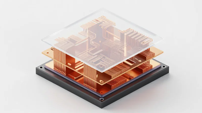
The Mechanics of Sequential Lamination
Sequential lamination is an iterative fabrication process used to create complex, high-density interconnect (HDI) boards. Unlike standard multi-layer boards where all layers are bonded simultaneously, sequential lamination involves building up the circuit board in stages. An inner core is laminated, drilled, and plated, and then additional layer pairs are added and laminated in subsequent cycles. This process is the foundational technology that enables the use of blind and buried vias, allowing for sophisticated routing density that would be impossible with traditional through-hole manufacturing.
Impact on Tolerance Stack-ups
Because each lamination cycle exposes the materials to high temperatures and mechanical pressures, the dielectric substrates undergo expansion and contraction repeatedly. This creates cumulative registration errors. Designers must account for 'layer shifting' during the design phase, as the alignment between layer groups can deviate more significantly than in standard processes. Failure to design with these registration tolerances in mind often leads to open circuits or shorted vias during the fabrication of sub-assemblies.
| Feature | Standard Lamination | Sequential Lamination |
|---|---|---|
| Lamination Cycles | Single | Multiple |
| Registration Complexity | Low | High |
| Cost Implications | Lower | Higher |
| Design Flexibility | Limited | High (HDI) |
| Via Types | Through-hole | Blind/Buried |
Why Early DFM is Non-Negotiable
In sequential lamination, the 'Design for Manufacturing' (DFM) phase is not merely an optional review—it is a critical engineering requirement. Errors in pad sizing or via-to-trace clearance that might be overlooked in standard boards will result in catastrophic yield loss here. Early collaboration with your fabricator is mandatory to align your stack-up with their specific manufacturing tolerances.
- How does lamination cycle count affect cost?
Each additional lamination cycle adds significant cost due to additional drilling, plating, and bonding steps. Reducing the number of required cycles is a primary objective in cost-optimized HDI design. - Why is drill-to-copper alignment critical?
Because layers are added and processed at different times, the registration between the initial core and outer layers is prone to drift. Robust annulus rings are required to compensate for this mechanical shifting. - Can I mix blind and buried vias freely?
No; they must be placed strategically to align with specific lamination steps. A buried via can only exist within the specific sub-stack it was drilled for during the early stages of the build.
Optimizing Layer Stack-up for Structural Integrity
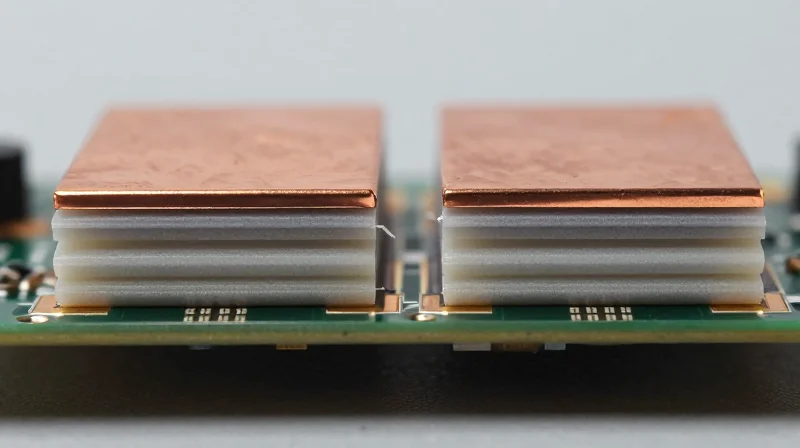
The structural integrity of a high-density interconnect (HDI) board is primarily determined by the symmetry of its stack-up. In sequential lamination, the board undergoes multiple heat and pressure cycles, making it highly susceptible to mechanical instability. Maintaining a balanced layup—where copper weight, dielectric thickness, and material composition are mirrored across the board's neutral axis—is critical to preventing warpage, twisting, and delamination.
Principles of Balanced Construction
A balanced stack-up ensures that the thermal expansion forces generated during the lamination process act equally on both sides of the board. Neglecting this leads to uneven coefficient of thermal expansion (CTE) stresses, which cause permanent warping that can complicate assembly and affect via reliability.
| Parameter | Best Practice | Consequence of Imbalance |
|---|---|---|
| Copper Distribution | Uniform density across all layers | Differential stress leading to warping |
| Dielectric Thickness | Mirror materials relative to centerline | Impedance deviation and bowing |
| Lamination Cycle | Balanced heating profiles | Inter-layer registration misalignment |
FAQs on Structural Integrity
- How does copper weight affect stack-up stability?
Uneven copper weight distribution creates localized zones of varying thermal mass, which expand at different rates, directly resulting in board bow and twist. - Can I use different dielectric materials in one stack-up?
Avoid mixing different core/prepreg material types in a stack-up as they possess different CTE values; always maintain material symmetry to keep the board flat. - Why does impedance fluctuate in HDI designs?
Impedance shifts often occur due to inconsistent resin flow during lamination; symmetric stack-ups help distribute resin pressure evenly, ensuring predictable dielectric thickness.
Always consult with your fabricator early in the design phase to align your stack-up with their specific lamination equipment capabilities. A design that is theoretically balanced may still experience issues if the manufacturer's lamination press cannot accommodate the specific material flow requirements of your layer geometry.
Micro-via Aspect Ratio Constraints
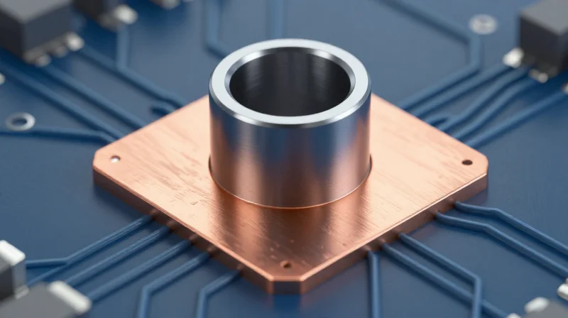
Defining the Micro-via Aspect Ratio
The aspect ratio of a micro-via is defined as the ratio of its depth (the thickness of the dielectric layer) to its diameter. In high-density interconnect (HDI) designs, keeping this ratio within manufacturing limits is critical; exceeding the ratio makes it nearly impossible for electroplating solutions to penetrate the via, resulting in voids, thin barrel walls, and eventual field failures due to barrel cracking.
| Via Technology | Recommended Max Aspect Ratio | Primary Risk |
|---|---|---|
| Laser Drilled (Micro-via) | 0.75:1 to 1:1 | Plating voids/Copper thinning |
| Mechanical Drilled | 8:1 to 10:1 | Drill wander and wall roughness |
| Stacked Micro-via | 0.75:1 (per layer) | Thermal stress/barrel separation |
Critical Reliability Factors
When designing for micro-vias, it is essential to account for the thickness of the prepreg layers. Thicker dielectrics require larger capture pads to maintain a viable aspect ratio, which in turn consumes valuable routing area. If a design demands a specific via depth, fabricators often prefer thin-core materials to maintain the 1:1 ratio threshold, ensuring that the copper plating can effectively reach the bottom of the hole.
Frequently Asked Questions on Via Geometry
- Why is a 1:1 ratio considered the industry standard?
A 1:1 ratio balances the need for high density with the physics of chemical plating; exceeding this ratio creates a 'high-aspect' scenario where gas bubbles trapped in the via prevent copper deposition. - How does aspect ratio affect thermal cycling?
Lower aspect ratios create more robust copper barrels that resist the Z-axis expansion of the PCB substrate during solder reflow, preventing the fatigue cracks common in high-aspect-ratio holes. - Can stacked vias improve density?
Yes, but they are significantly more sensitive to aspect ratio constraints. Each via in the stack must independently meet the fabricator's limit, and they require specialized copper-filled plating processes to prevent hollow interfaces.
Precision Drill Depth and Registration Control
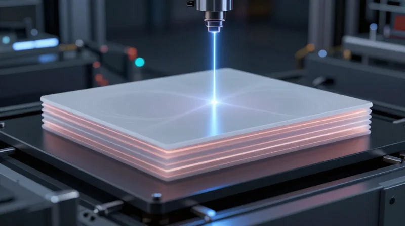
Managing Drill Depth Accuracy
Depth-controlled drilling is the cornerstone of successful blind via formation. Because standard mechanical drills have inherent tolerance variations, the industry relies heavily on laser ablation for blind vias that terminate on internal layers. To ensure the drill reaches the target landing pad without penetrating too deep—or failing to make electrical contact—designers must specify sufficient capture pad sizes and maintain strict dielectric thickness tolerances across the board's surface.
Strategies for Registration Stability
Registration errors compound during sequential lamination cycles due to material movement and thermal expansion. To combat this, employ optimized tooling hole placement and prioritize board features that allow for x-ray alignment during the drilling phase.
| Registration Factor | Control Strategy | Impact on Yield |
|---|---|---|
| Material Shrinkage | Pre-bake and material compensation | High (prevents misalignment) |
| Tooling Holes | Optical alignment via X-ray | Critical (ensures pad capture) |
| Copper Distribution | Balanced internal pattern design | Medium (reduces thermal stress) |
Frequently Asked Questions
- Why is laser drilling preferred over mechanical drilling for blind vias?
Laser drilling offers superior depth control and the ability to stop consistently on copper surfaces, whereas mechanical drilling is limited by bit deflection and depth tolerance issues at high aspect ratios. - How does layer count impact registration drift?
Each additional lamination cycle increases the potential for cumulative registration error; using symmetrical stack-ups and balanced copper distribution helps equalize the internal stresses that drive this movement. - What is the recommended clearance for capture pads?
To accommodate drilling registration tolerances, a minimum annular ring of 50-75 microns is generally recommended, depending on the specific HDI class and fabrication capabilities of your vendor.
Managing Signal Integrity and Via Stubs
The Impact of Via Stubs on Signal Integrity
In multilayer PCB designs, a via stub is the unused portion of a via that remains after a signal path has changed layers. At high frequencies, these stubs act as unterminated transmission line segments, creating resonant stubs that lead to signal reflections, increased insertion loss, and severe eye diagram degradation. Controlling stub length is essential for maintaining signal integrity, particularly in data rates exceeding 10 Gbps.
Comparison of Via Configurations
| Via Type | Stub Presence | High-Speed Suitability |
|---|---|---|
| Through-hole | Maximum | Poor |
| Blind Via | Minimal | Good |
| Buried Via | None | Excellent |
| Back-drilled Via | Near Zero | Excellent |
Strategic Mitigation Techniques
To minimize parasitic capacitance and inductance, designers must utilize specific routing and manufacturing strategies. Reducing stub length through optimized stack-up planning or physical removal via post-fabrication processes is industry standard for high-bandwidth applications.
- How does back-drilling improve signal integrity?
Back-drilling involves using a controlled-depth drill bit to remove the copper plating from the unused portion of a through-hole via, effectively eliminating the stub and its associated resonance. - What is the maximum recommended stub length?
While it depends on the signal edge rate, a common design rule is to limit stub length to less than 20-25 mils for frequencies above 5 GHz to avoid reaching the quarter-wave resonant frequency. - Why prefer buried vias for high-speed signals?
Buried vias are encapsulated within the inner layers of the PCB, meaning they do not create stubs that extend to the external board surfaces, resulting in zero parasitic reflection from stub effects.
Design Guidelines for Stub Management
Designers should prioritize placing signal transitions on adjacent layers whenever possible to reduce total via length. When blind or buried vias are implemented, ensure that the drilling aspect ratio is respected to allow for high-quality, uniform copper plating, which further stabilizes the impedance of the signal path.
Common Manufacturing Defects and Prevention
Frequent Manufacturing Defects in HDI Boards
Manufacturing multi-layer HDI boards with laser-drilled blind and buried vias presents unique challenges, primarily involving alignment, chemical deposition, and material integrity. Defects such as via breakout, incomplete dielectric filling, and plating voids often stem from mismatched registration tolerances or aggressive drilling parameters that exceed the substrate's mechanical capabilities.
| Defect Type | Primary Root Cause | Prevention Strategy |
|---|---|---|
| Via Breakout | Layer misalignment | Increase annular ring size; utilize advanced optical registration. |
| Plating Voids | Inadequate desmear or aspect ratio | Optimize drill parameters; improve plasma etch processes. |
| Incomplete Resin Fill | Excessive viscosity; high aspect ratio | Ensure proper dielectric flow properties; utilize sequential lamination. |
Prevention and Design Best Practices
- How can I prevent via breakout during the drilling process?
Implement larger annular ring requirements for your specific HDI class and coordinate with your fabricator to understand their registration tolerance limits for laser-drilled features. - Why does incomplete dielectric flow occur in buried vias?
This is often caused by high-viscosity prepreg or vias placed too close together. Designing with adequate spacing and choosing flow-optimized materials mitigates air entrapment. - What is the best way to avoid copper plating voids?
Ensure the drill aspect ratio is within the manufacturer's certified limits and enforce a rigorous desmear process to remove resin debris that prevents consistent copper deposition. - Should I use via-in-pad for all blind vias?
While via-in-pad is common for HDI, ensure the vias are properly plugged and capped (VIPPO) to prevent solder wicking and surface flatness issues during assembly.
Ultimately, the key to successful DFM for blind and buried vias lies in proactive communication with your PCB vendor. By aligning your design constraints with the fabricator's specific process capabilities early in the layout phase, you minimize the risk of yield-killing defects.
Leveraging CAM Tools for DFM Verification

The Role of CAM Tools in DFM Verification
While CAD software provides the design environment, CAM (Computer-Aided Manufacturing) tools act as the final gatekeeper by simulating the actual manufacturing process. By importing Gerber, ODB++, or IPC-2581 data into advanced CAM suites like UCAMco or Valor, engineers can perform comprehensive DFM analysis that identifies potential issues—such as annular ring violations or drilling registration offsets—before they reach the shop floor.
Critical DFM Checkpoints for Blind and Buried Vias
| Check Category | Target Analysis | Risk Mitigation |
|---|---|---|
| Annular Ring | Verification of registration at all drill spans. | Prevent breakout on inner layers. |
| Aspect Ratio | Calculates hole diameter vs. dielectric stackup thickness. | Ensures reliable copper plating coverage. |
| Staggered Vias | Analyzes relative proximity of stacked via structures. | Avoids excessive dielectric stress during thermal cycles. |
Best Practices for Pre-Manufacturing Validation
- Why should I use ODB++ instead of Gerber files?
ODB++ maintains a hierarchical, intelligent database of the design, which prevents data misinterpretation during the CAM import process and ensures stackup integrity. - How does automated netlist comparison help?
Automated netlist comparison verifies that the generated artwork exactly matches the intended design netlist, identifying accidental shorts or opens created during manual copper pours. - When is the ideal time to run DFM analysis?
DFM checks should be run iteratively during the routing phase, with a final full-suite verification conducted immediately after the final design freeze.
To streamline this workflow, integrate DFM script execution directly into your design release pipeline. Automated scripts can scan for specific blind/buried via constraints, such as ensuring that the micro-via landing pads meet the required copper weight-to-drill aspect ratio standards, thereby reducing communication cycles with your PCB fabricator.
Collaboration: Communicating with Your PCB Fabricator
Early-Stage Stack-up Consultation
The most significant errors in blind and buried via designs often stem from assumptions made before the fabrication process begins. Engaging your fabricator during the initial stack-up definition phase is not optional; it is the most effective way to prevent costly design revisions. Fabricators possess specific internal capabilities regarding laser drilling aspect ratios, registration tolerances, and dielectric material availability that directly influence the viability of your via structure.
Key Data Points for Fabrication Approval
| Data Requirement | Strategic Benefit | Risk if Omitted |
|---|---|---|
| Copper Weights | Ensures precise impedance matching | Etch compensation failure |
| Dielectric Material | Aligns with press cycles | Delamination or registration drift |
| Via Span Definitions | Confirms laser capability | Unmanufacturable aspect ratio |
Essential Fabrication Documentation
Generic fabrication notes are insufficient for complex multilayer boards utilizing blind and buried vias. You must provide a comprehensive fabrication drawing that explicitly details the drill layers, required surface finishes, and controlled impedance constraints. Ambiguity in these documents forces fabricators to make assumptions, which often leads to the rejection of the design files.
Frequently Asked Questions for Fabricator Collaboration
- Why must I share my Gerber files before formal sign-off?
Sharing preliminary data allows the fabricator to run a DFM analysis that identifies potential issues with drill-to-copper spacing or annular ring widths early in the cycle. - What specific details regarding blind vias are most vital?
Always specify the start and end layer pairs, the drilling method (mechanical vs. laser), and whether the vias must be filled or capped. - How does stack-up symmetry affect manufacturing?
Balanced stack-ups prevent board warping during lamination; fabricators can suggest material pairings to maintain this structural integrity.
Mastering the complexities of blind and buried vias is not just about avoiding errors; it is about enabling superior performance in modern electronics. By adhering to these DFM principles, you ensure your designs are production-ready from day one. Contact our engineering team today to review your current stack-up and optimize your next high-performance PCB layout.
