
In the fast-paced world of Industrial IoT, a sensor node that fails on the factory floor is more than a technical inconvenience; it is a costly operational bottleneck. Achieving true manufacturing excellence requires more than standard design—it demands a rigorous commitment to Design for Manufacturing (DFM) principles specifically engineered for harsh environments. In this guide, we dive deep into the technical strategies that transform fragile prototypes into resilient, field-hardened industrial assets.
Understanding the Demands of Industrial Environments
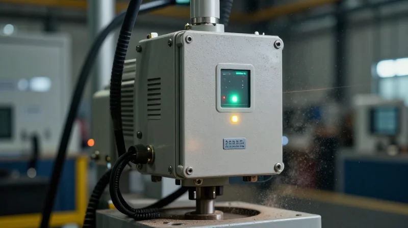
Industrial environments are defined by their unpredictability and harshness. Unlike consumer-grade electronics, industrial IoT (IIoT) sensor nodes are subjected to constant mechanical fatigue, thermal cycling, and chemical degradation. Mastering DFM for these devices requires an upfront acknowledgement that hardware survival depends on material selection, enclosure integrity, and component placement that minimizes internal stress.
Key Environmental Stressors
| Stressor | Primary Impact | Design Consideration |
|---|---|---|
| Temperature Extremes | Component failure, solder joint cracks | Wide temp-rated (-40C to 85C) ICs |
| High Vibration | Interconnect failure, fatigue | Conformal coating, thread lockers |
| Chemical Exposure | Corrosion, trace oxidation | IP67-rated seals, inert materials |
Common Implementation Questions
- How does vibration affect long-term reliability?
Continuous high-frequency vibration can lead to work hardening in solder joints and the loosening of fasteners, eventually creating intermittent electrical shorts or open circuits. - Why is thermal management critical for IIoT?
Thermal expansion mismatches between the PCB substrate and soldered components cause mechanical stress during cycling, leading to premature fatigue and eventual interconnect failure. - Are standard enclosures sufficient for industrial sites?
No, standard off-the-shelf enclosures often fail in chemically volatile or high-particulate environments, necessitating IP-rated housings with chemical-resistant gaskets and pressure-equalization vents.
Engineers must validate designs using accelerated life testing (ALT) early in the prototyping phase. Incorporating high-reliability assembly practices—such as underfilling BGA packages and using vibration-dampening standoffs—is not merely optional, but a mandatory requirement for operational longevity in the factory ecosystem.
Strategic Substrate Selection for Extreme Conditions
Critical Material Properties for Extreme Environments
In industrial IoT applications, the substrate is not merely a carrier but a structural component that must maintain mechanical stability across a wide temperature spectrum. Designers must prioritize high glass transition temperature (Tg) materials to prevent the dielectric from softening and becoming chemically reactive at peak operating temperatures. Simultaneously, the coefficient of thermal expansion (CTE) must be closely matched to the surface-mount component packages to mitigate fatigue in solder joints during repeated thermal expansion and contraction cycles.
| Material Property | Industrial Requirement | Impact on Reliability |
|---|---|---|
| Glass Transition (Tg) | > 170°C | Prevents delamination and Z-axis expansion during reflow. |
| CTE (X/Y Axis) | 12-16 ppm/°C | Reduces stress on copper traces and vias. |
| Decomposition Temp (Td) | > 325°C | Ensures structural integrity under localized overheating. |
Substrate Selection Best Practices
- Why should I avoid standard FR-4?
Standard FR-4 often features a Tg around 130-140°C, which is insufficient for industrial nodes exposed to rapid thermal cycling, leading to fractured via barrels and delamination. - How does CTE matching protect solder joints?
By selecting substrates with a CTE close to ceramic or silicon packages, the difference in expansion rates is minimized, significantly reducing the shear force applied to solder interconnects during temperature fluctuations. - Are halogen-free materials recommended?
Yes, high-Tg, halogen-free laminates offer superior thermal stability and moisture resistance, making them ideal for deployments in humid or corrosive industrial environments.
Advanced Thermal Management Strategies
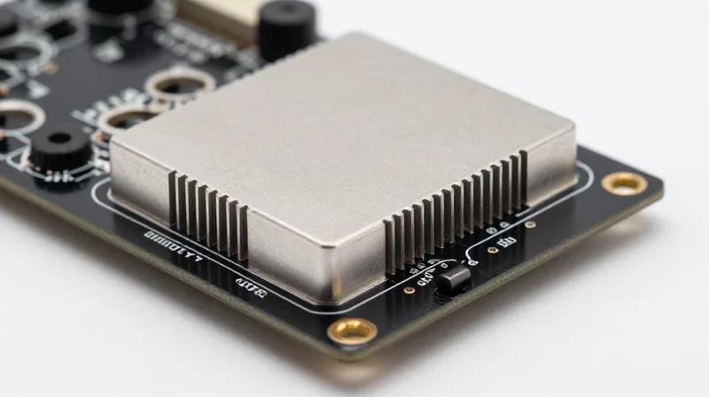
Advanced Thermal Management Strategies
For industrial IIoT nodes, thermal management is not merely about cooling; it is about managing the path of least resistance for heat to move from high-power density components into the environment. As sensor nodes shrink, the reliance on passive cooling techniques like thermal vias and dedicated copper dissipation planes becomes essential for preventing semiconductor degradation and maintaining signal integrity.
Optimizing Heat Dissipation Paths
Modern PCB design for IIoT demands a holistic approach to heat sinking. By utilizing internal copper layers as heat spreaders and maximizing the efficacy of thermal vias through direct connection to chassis-ground heat sinks, designers can significantly lower the junction temperature of critical microcontrollers and radio modules.
| Thermal Method | Primary Function | DFM Recommendation |
|---|---|---|
| Thermal Vias | Vertical heat transfer | Use a 0.2mm diameter pitch with conductive epoxy fill. |
| Copper Pours | Lateral heat spreading | Ensure large, unbroken planes connected to thermal pads. |
| TIM Application | Interface gap filling | Use high-conductivity phase change materials for vibration. |
Frequently Asked Questions on Thermal Reliability
- How do thermal vias affect PCB assembly?
Improperly sealed thermal vias can lead to solder wicking, which creates voids under components; use via-in-pad plating or epoxy capping to prevent this. - When is an external heat sink mandatory?
An external heat sink is required when the calculated junction-to-ambient thermal resistance (θJA) cannot be sufficiently lowered by PCB-level copper dissipation alone. - Does high thermal conductivity material increase cost?
Yes, high-Tg or ceramic-filled substrates increase BOM costs but are essential for preventing delamination in environments exceeding 100°C.
Designing Robust Solder Joints
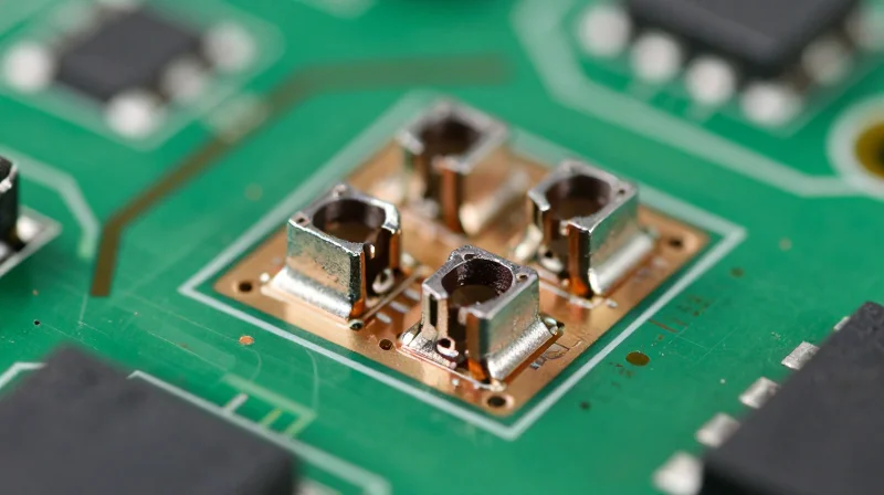
Optimizing Solder Joint Geometry
The mechanical integrity of a solder joint is primarily determined by its geometry, which dictates how stresses from thermal expansion and mechanical loads are distributed. For industrial sensor nodes, a concave fillet is ideal for SMT components as it provides optimal stress distribution, whereas excessive solder (convex fillets) can create stress concentrations that promote cracking.
Alloy Selection for Vibration and Shock Resistance
In industrial IoT applications, the choice of solder alloy is critical. While SAC305 is the industry standard, it may struggle with high-vibration environments due to its relative brittleness. High-reliability alloys containing bismuth, indium, or antimony are often preferred for their enhanced ductility and vibration dampening capabilities.
| Alloy Type | Primary Application | Key Advantage |
|---|---|---|
| SAC305 | Standard Industrial IoT | Excellent wetting and availability |
| Innolot | High Vibration/Shock | High creep resistance and ductility |
| SAC-Bi | Automotive/Heavy Industrial | Improved fatigue life in thermal cycling |
DFM Considerations for Long-Term Reliability
- How does component size impact joint failure?
Larger components experience greater shear strain during thermal cycling due to CTE mismatches. Minimize the use of large BGA packages in high-vibration zones unless advanced underfill is applied. - Why is solder mask defined (SMD) vs non-solder mask defined (NSMD) important?
NSMD pads are generally preferred for BGA components as they allow solder to wrap around the pad sides, providing a stronger mechanical anchor against shock compared to SMD pads. - What role does underfill play?
Underfill redistributes mechanical stresses from the solder joints to the PCB surface, significantly increasing the fatigue life of high-I/O count components in rugged environments.
Component Placement and PCB Layout Optimization

Optimizing PCB layout for industrial IoT involves balancing electrical performance with mechanical durability. By carefully managing component placement, engineers can mitigate stress, prevent interference, and facilitate consistent, high-yield automated assembly processes.
Critical Placement Rules for Mechanical Integrity
Components must be positioned to avoid localized strain during PCB flexing or vibration. Large, heavy components—such as electrolytic capacitors, inductors, and connectors—are particularly susceptible to mechanical failure if placed near board edges or mounting holes.
- Proximity to Board Edges
Avoid placing sensitive or rigid components within 5mm of the PCB edge to prevent stress fractures during panel depaneling or housing installation. - Connector Stress Management
Place connectors away from high-flex areas; add mechanical support or anchoring holes if the connector is subject to frequent mating force. - Symmetry and Balance
Distribute high-mass components evenly across the board to prevent warping during reflow soldering and to ensure structural balance.
Assembly Yield and Clearance Optimization
Adherence to strict clearance standards is required for automated optical inspection (AOI) and rework accessibility. The table below summarizes recommended layout strategies for maximizing assembly yield.
| Design Factor | Recommended Practice | Reasoning |
|---|---|---|
| Component Clearance | Min 0.5mm (SMD to SMD) | Prevents solder bridging and allows repair access. |
| Trace Routing | Keep traces off board edges | Minimizes exposure to copper oxidation and shorts. |
| Fiducials | 3 fiducials per board | Ensures precise alignment for high-speed pick-and-place. |
| Test Points | Solder mask excluded | Enables reliable ICT (In-Circuit Testing) connectivity. |
Managing Thermal and Electrical Crosstalk
Sensor nodes often pack high-frequency communication modules alongside sensitive analog acquisition circuitry. Effective DFM requires physical segregation of these zones to prevent thermal coupling and electromagnetic interference (EMI). Place decoupling capacitors as close to power pins as possible, and route high-speed digital signals away from high-impedance analog sensor traces to maintain signal integrity in noisy industrial environments.
Protective Measures: Conformal Coating and Potting
Protective Barriers for Industrial Longevity
Deploying IoT sensor nodes in industrial settings—often characterized by high humidity, corrosive gases, and temperature fluctuations—necessitates robust chemical and physical barriers. Conformal coating provides a thin, protective layer that seals components against environmental contaminants, while potting compounds offer a comprehensive encapsulant solution, providing superior structural integrity and defense against vibration and chemical ingress.
Selecting the Right Protection Strategy
| Feature | Conformal Coating | Potting |
|---|---|---|
| Application | Spraying, dipping, or brushing | Encapsulation in a housing |
| Thickness | Very thin (10-100 microns) | Thick (enclosed volume) |
| Primary Benefit | Moisture/Dust resistance | Extreme shock/vibration resistance |
| Weight Impact | Negligible | Significant increase |
Key Design Considerations for Application
- How does component density affect coating application?
High component density can lead to shadowing effects, where the coating fails to penetrate under low-profile components. Design layouts with sufficient clearance to ensure coverage and prevent 'keep-out' zones that might interfere with manual or robotic application. - What should be considered regarding thermal expansion?
Potting compounds have high thermal mass. Ensure the Coefficient of Thermal Expansion (CTE) of your potting resin is matched to the components it surrounds; otherwise, thermal cycling may cause the compound to crack or delaminate from delicate solder joints. - Which areas must remain free of chemical protection?
Connectors, sensitive MEMS microphones, pressure ports, and light-emitting elements must be masked during application to prevent functional impairment or signal degradation.
When selecting materials, prioritize options with low-volatile organic compound (VOC) emissions for electronics assembly. Furthermore, ensure that the chosen coating or potting compound is compatible with board-level cleaning agents to prevent chemical residue interaction, which can lead to long-term electrochemical migration or dendrite growth.
DFM Verification and Design Validation Testing
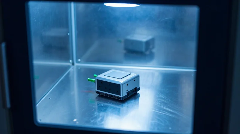
The Necessity of Early-Stage Validation
Design for Manufacturing (DFM) verification is incomplete without aggressive physical validation. For IIoT sensor nodes, which often reside in harsh industrial environments, standard functional testing is insufficient. You must implement stress-based testing to expose latent design flaws, such as solder joint vulnerabilities or thermal management inefficiencies, that only emerge under extreme operational conditions.
Key Testing Protocols for Reliability
| Test Method | Primary Objective | IIoT Application |
|---|---|---|
| HALT (Highly Accelerated Life Testing) | Identify failure limits through thermal/vibration stress | Accelerated aging validation |
| HASS (Highly Accelerated Stress Screening) | Production screening to catch infant mortality | Quality control during assembly |
| Thermal Cycling | Verify coefficient of thermal expansion (CTE) mismatches | Outdoor/industrial temperature swings |
Implementing HALT in DFM Cycles
HALT is not merely a test; it is a discovery process. By applying multi-axis vibration and rapid thermal cycling simultaneously, you can compress years of environmental exposure into days. For IIoT hardware, focus your HALT efforts on critical failure points: BGA interconnects, electrolytic capacitors, and conformal coating integrity. If a design fails during HALT, the resulting data provides a forensic roadmap for DFM adjustments, such as modifying trace routing or reinforcing mechanical mounting points.
Frequently Asked Questions
- At what stage should HALT be introduced?
HALT should be conducted on high-fidelity prototypes immediately after the initial DFM iteration to ensure structural integrity before committing to expensive production tooling. - Is HASS necessary for every production unit?
HASS is typically reserved for critical-mission nodes where failure could result in significant safety risks or massive downtime, serving as a screen for manufacturing defects rather than design flaws. - How do I correlate test results with field life?
Utilize acceleration factors derived from the Arrhenius model for thermal stress and Coffin-Manson models for mechanical fatigue to translate test hours into estimated field operational years.
Building for the industrial edge requires a proactive approach to engineering where reliability is designed in from the first trace. By mastering these DFM principles, you ensure your sensor nodes deliver consistent performance regardless of the environment. Ready to optimize your hardware for the factory floor? Contact our engineering team today for a comprehensive design review.
