
In the fast-evolving landscape of medical robotics, the marriage of high-speed vision processing and precision motor control is the heartbeat of innovation. Engineers face the daunting task of balancing signal integrity, thermal management, and strict regulatory compliance. This article provides a comprehensive blueprint for mastering DFM principles to ensure your next-generation motherboard delivers flawless performance in critical healthcare environments.
The Anatomy of a High-Speed Medical Motherboard
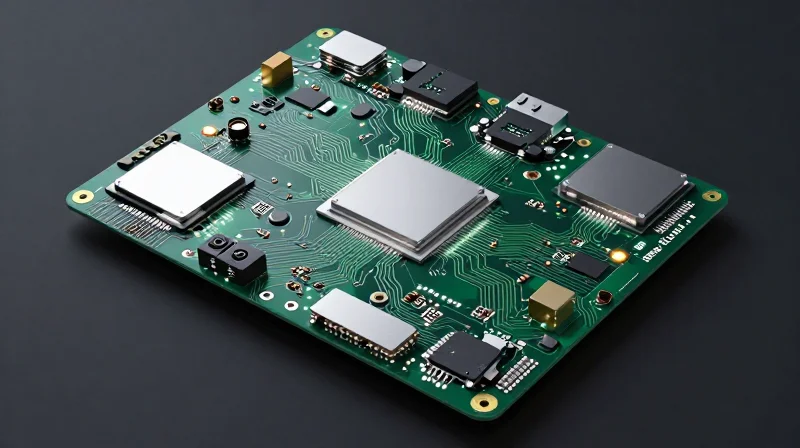
Architectural Foundation for Hybrid Processing
To achieve high performance, modern telemedicine PCBs must decouple the high-throughput processing required for real-time vision algorithms from the precise, deterministic requirements of motion control. This separation is typically managed through a heterogeneous computing architecture utilizing SoCs (System-on-Chip) or FPGAs paired with high-performance real-time microcontrollers. The motherboard design must ensure signal integrity across these domains to prevent high-frequency EMI from disrupting sensitive motor feedback loops.
Resource Allocation and Signal Integrity
| Feature | Vision Processing Domain | Motion Control Domain |
|---|---|---|
| Primary Requirement | High Bandwidth / Throughput | Deterministic Latency |
| Signal Routing | Controlled Impedance Differential Pairs | Shielded Traces / Low-Pass Filtering |
| Component Focus | FPGAs, GPUs, DDR4/5 Memory | Real-time MCUs, Isolated Gate Drivers |
Key Design Considerations for DFM
- How do we mitigate crosstalk between vision and motion systems?
Implement physical board partitioning with dedicated ground planes and strict keep-out zones for high-speed differential pairs, ensuring that switching noise from motor drivers does not couple into high-resolution vision sensor interfaces. - Why is thermal management critical for these specific motherboards?
Vision processing units generate significant localized heat which can cause thermal drift in motion feedback sensors; DFM strategies must include strategic copper pouring and thermal vias to ensure consistent operating temperatures across the board. - What role does stack-up design play in reliability?
A minimum 8-to-12 layer stack-up is essential to provide adequate return paths and impedance control, which prevents jitter in motion commands and frame drops in high-speed vision pipelines.
Strategic Layer Stack-up for Signal Integrity
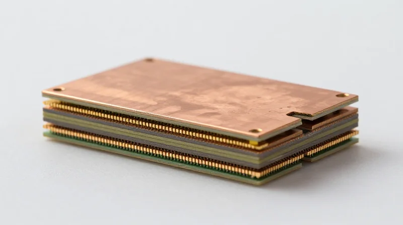
Optimizing Stack-ups for Mixed-Signal Integrity
Achieving signal integrity in telemedicine systems requires a balanced stack-up design that isolates high-speed data lanes from sensitive motor control signals. By employing a primary reference plane strategy—typically utilizing ground planes adjacent to signal layers—designers can effectively manage impedance control and minimize return path inductance, which is critical when synchronizing high-resolution vision data with sub-millisecond motion feedback.
Layer Configuration Best Practices
| Layer Function | Design Priority | Mitigation Strategy |
|---|---|---|
| High-Speed Differential Pairs | Impedance Continuity | Keep reference planes continuous; avoid splits. |
| Motion Control/PWM | Crosstalk Reduction | Increased spacing and guard traces. |
| Sensitive Analog/Sensor | Noise Immunity | Use dedicated quiet zones and isolation trenches. |
Frequently Asked Questions
- How do I prevent vision processing noise from affecting motion control?
Implement physical layer separation using internal ground shielding and ensure that high-frequency data paths are routed on layers internal to the board, sandwiched between reference planes. - Is a six-layer stack-up sufficient for medical imaging systems?
While possible, an eight-layer or higher stack-up is generally recommended to provide dedicated reference planes for every signal layer, which significantly reduces EMI and improves return path management. - What is the impact of via stubs on high-speed signals?
Via stubs create impedance discontinuities that can cause reflections in high-bandwidth vision streams; back-drilling or blind vias should be used to eliminate these stubs in high-speed segments.
Optimizing High-Density Interconnects (HDI)
Achieving Density with Micro-via Technology
In telemedicine hardware, where vision processing units and motion controllers must coexist on a single substrate, High-Density Interconnect (HDI) is not merely an option but a requirement. By utilizing laser-drilled micro-vias, designers can move away from traditional through-hole footprints, freeing up routing channels and reducing parasitic capacitance that compromises high-speed signal integrity.
| Via Type | Fabrication Method | Best Use Case | Reliability Impact |
|---|---|---|---|
| Through-Hole | Mechanical Drill | Power/Ground Planes | Low (High Aspect Ratio) |
| Blind Micro-via | Laser Ablation | BGA Escape Routing | High (Consistent) |
| Buried Via | Sequential Lamination | Internal Layer Routing | Moderate (Process Complex) |
Reliability Considerations for Medical-Grade HDI
Reliability in telemedicine depends on strict adherence to DFM standards during HDI implementation. As trace widths shrink to sub-3-mil dimensions, the risk of copper etching defects and dielectric breakdown increases. Employing sequential lamination allows for tighter registration control, but it introduces stress points at the micro-via interfaces; thus, utilizing 'staggered' rather than 'stacked' vias is recommended to distribute mechanical strain more effectively.
Frequently Asked Questions
- How does HDI influence thermal management in telemedicine units?
Increased routing density limits the copper surface area available for heat dissipation, necessitating the use of thermal vias under ICs and strategically placed thermal planes to prevent localized hot spots near motion control drivers. - Are there specific aspect ratio limits for laser-drilled vias?
To maintain reliable plating in a high-density medical PCB, keep the aspect ratio of micro-vias at or below 0.75:1 to avoid 'barrel cracking' during thermal cycling. - Should I use via-in-pad technology for vision processing chips?
Yes, via-in-pad is essential for high-pin-count FPGAs and processors, provided the vias are planarized or filled with conductive epoxy to prevent solder wicking and ensure stable joint formation.
EMI Shielding Techniques for Noise-Sensitive Environments
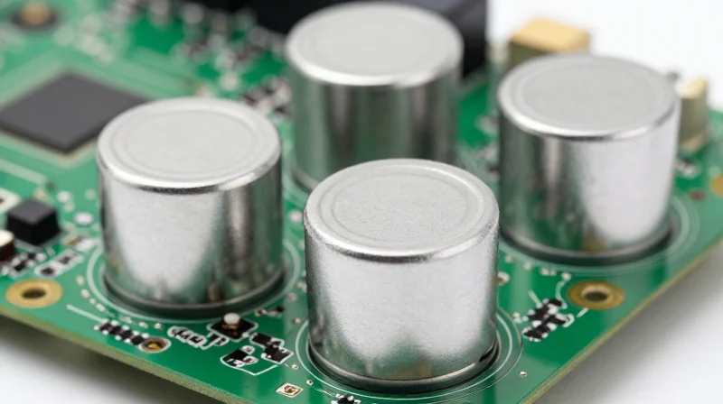
Isolating Vision Data from Motor-Induced Noise
In telemedicine systems, motor controllers create significant low-frequency magnetic interference, while high-speed vision interfaces (e.g., MIPI CSI-2 or LVDS) are inherently sensitive to jitter induced by electromagnetic radiation. To protect signal integrity, designers must implement a combination of physical compartmentalization, specialized component-level shielding, and rigorous differential pair routing to minimize the effective loop area of sensitive traces.
Strategic Shielding Methodologies
| Shielding Strategy | Primary Application | Implementation Note |
|---|---|---|
| Board-Level Shielding (BLS) | Sensor Interface/FPGA | Use multi-compartment cans to isolate noisy converters from quiet sensors. |
| Guard Traces | Differential Pairs | Ground-stitched guard traces provide high-frequency return paths and EMI suppression. |
| Faraday Caging via Vias | High-speed digital signals | Implement via fencing around sensitive traces to contain radiated emissions. |
Design Guidelines for EMI Mitigation
- How does via fencing mitigate noise?
Stitching ground vias along the perimeter of sensitive traces forms a Faraday cage that contains electromagnetic emissions and prevents crosstalk from high-current motor drive loops. - Where should Board-Level Shielding (BLS) be positioned?
BLS should be placed over sensitive analog-to-digital converters and high-speed data processors, ensuring physical separation between these zones and the pulse-width modulation (PWM) stages of motion controllers. - Why is reference plane continuity essential?
Breaks in the reference plane beneath high-speed signals force return currents to travel through high-impedance paths, increasing loop area and making the signals susceptible to external EMI injection.
Grounding Architecture and Decoupling
Proper grounding is the final line of defense against interference. For telemedicine PCBs, implement a 'star grounding' strategy at the power entry point while maintaining a continuous ground plane for data signals. Decoupling capacitors must be placed as close as possible to the IC power pins, using high-frequency ceramic capacitors (0201 or 0402 footprints) to bypass transients generated by high-torque motor bursts, effectively silencing the power rail before it reaches sensitive vision processing components.
Thermal Management in Compact Robotic Enclosures
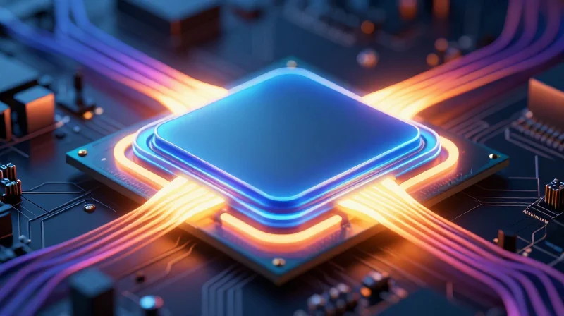
In telemedicine systems, the integration of high-resolution vision processing and motion control creates localized thermal hotspots that can trigger thermal throttling or premature component failure. Because robotic enclosures are typically sealed to facilitate sterilization, convection is limited. Engineers must prioritize thermal path design through DFM (Design for Manufacturing) by utilizing the PCB itself as a primary heat-spreading medium and integrating conductive paths directly into the mechanical housing.
PCB-Level Thermal Mitigation Strategies
To move heat away from sensitive ICs, the PCB layout must facilitate efficient thermal conduction. This involves increasing copper pour density, utilizing heavy copper inner layers, and strategically placing thermal vias in pad arrays. Connecting high-power motion controller drivers to ground planes via an array of stitched vias effectively turns the board into a large-surface-area heat sink.
| Thermal Technique | Implementation Strategy | Primary Benefit |
|---|---|---|
| Thermal Vias | Filled/capped vias in pad | Vertical heat dissipation to inner planes |
| Copper Pour | Maximize area on signal layers | Lateral heat distribution |
| Heat Pipes/Sinks | Direct contact via thermal interface material | Massive thermal mass management |
Frequently Asked Questions on Thermal DFM
- How do I manage heat in a fully sealed enclosure?
Utilize the robotic chassis as a passive heat sink by bridging components to the aluminum or magnesium housing using high-performance, electrically insulating thermal gap pads. - Does component placement affect thermal performance?
Yes, high-wattage motor drivers should be segregated from temperature-sensitive vision-processing FPGAs to prevent cross-component thermal coupling. - Should I use blind or buried vias for thermal management?
While primarily for density, thermal vias should ideally extend through the entire stack-up or connect directly to a high-copper-content ground plane to maximize conductive efficiency.
Managing Power Integrity for Mixed-Signal Systems
Managing Power Integrity for Mixed-Signal Systems
Achieving stable performance in mixed-signal telemedicine devices hinges on the effective isolation of high-energy motor control circuits from sensitive analog and digital vision processing pathways. When high-speed motion control creates current transients on the power plane, these ripples can couple into the sensitive logic rails, causing system jitter, image sensor artifacts, or erroneous data interpretation. Designers must prioritize local decoupling, star-grounding topologies, and physical separation to ensure electromagnetic compatibility (EMC) and signal integrity within a unified PCB architecture.
Isolation and Decoupling Strategies
| Strategy | Implementation Benefit | Key DFM Consideration |
|---|---|---|
| Split Power Planes | Isolates motor current spikes | Requires careful bridge management |
| Local Decoupling | Reduces high-frequency noise | Minimize loop inductance |
| Ferrite Beads | Filters high-frequency EMI | Check saturation current limits |
Best Practices for Power Distribution
- How should I structure the ground planes?
Utilize a star-grounding architecture to connect the motor-power return to the chassis or main power supply reference separately from the vision-system logic ground, preventing common-mode noise propagation. - What is the role of bulk versus high-frequency decoupling?
Use bulk capacitors (tantalum or electrolytic) at the entry point of the PCB for low-frequency stabilization, and place ceramic capacitors (0402 or 0201 packages) as close as possible to the IC power pins to handle high-frequency transients. - Can trace routing impact power stability?
Yes, high-current traces should be kept short and wide to minimize series inductance. Never route high-speed digital or analog signals beneath high-current motor pathways, as capacitive coupling will induce noise into the sensitive nets.
Regulatory Compliance and DFM Validation
Integrating IEC 60601-1 into the DFM Workflow
Achieving compliance for telemedicine robotics is not a post-production audit; it is a design-phase discipline. By embedding IEC 60601-1 requirements—specifically regarding creepage, clearance, and isolation—into the initial schematic and layout stages, engineers can prevent costly redesign cycles. Validation begins by establishing strict separation zones between high-power motion control circuitry and low-voltage vision processing components to satisfy dielectric strength requirements.
Critical Validation Metrics for Medical PCBs
| Requirement | DFM Validation Method | Compliance Objective |
|---|---|---|
| Creepage/Clearance | Automated DRC constraints | Patient electrical isolation |
| Thermal Stability | FEA simulation | Prevent component degradation |
| EMC/EMI Shielding | Near-field scanning | System signal integrity |
FAQ: Regulatory and Design Verification
- How does DFM simulation support IEC 60601-1 testing?
Design-phase simulations, such as thermal and EMI modeling, allow engineers to identify potential failure points in heat dissipation or electromagnetic emissions before physical prototypes are manufactured. - Why is isolation critical for motion-vision integration?
Telemedicine devices often interact directly with patients; robust galvanic isolation between the motor drives and the vision controller is mandatory to prevent fault currents from reaching user-accessible touchpoints. - What documentation is required for PCB design validation?
A complete Design History File (DHF) must include documented DFM rule checks, simulation results, and proof of trace isolation analysis to satisfy regulatory bodies during certification.
Future-Proofing Your Design Workflow

Implementing Modular Architecture for Rapid Iteration
To survive the rapid innovation cycle of medical robotics, engineers must move away from monolithic PCB designs. By adopting a modular approach, such as utilizing high-speed mezzanine connectors for vision processing modules or detachable motor driver sub-assemblies, you can upgrade specific system capabilities without redesigning the entire motherboard. This strategy significantly reduces time-to-market when hardware revisions become necessary due to new sensor standards or regulatory updates.
Scalable DFM Strategies
| Strategy | Benefit | Future-Proofing Impact |
|---|---|---|
| Standardized Footprints | Faster component swaps | Adapts to supply chain shifts |
| High-Density Interconnects | Reduced PCB real estate | Supports miniaturization trends |
| Simulation-Driven Design | Less physical prototyping | Ensures long-term signal integrity |
Design for Evolution: Common Challenges
- How do I ensure backward compatibility in future PCB revisions?
Utilize common power distribution rails and standardized I/O pin-outs to allow newer processor modules to interface with legacy motor control backplanes seamlessly. - Does component miniaturization compromise future repairs?
While smaller components like 0201 passives save space, incorporate larger test points and keep critical signals accessible on outer layers to facilitate easier diagnostic probing and firmware debugging in future iterations. - How does software-defined hardware affect my layout?
Design your PCB with extra FPGA logic resources and flexible GPIO routing. This allows for post-deployment updates to motion control algorithms or vision processing pipelines without physical board changes.
Successfully integrating high-speed vision with precision motion control requires more than just functional schematics; it demands a deep commitment to DFM rigor and electromagnetic precision. By implementing these strategies, your team can reduce development cycles and ensure the reliability medical professionals depend on. Contact our engineering team today to audit your current PCB designs and accelerate your time-to-market.
