
In the high-stakes world of modern electronics, Ball Grid Array (BGA) components are essential for high-density designs, yet they remain one of the most challenging elements to assemble correctly. Achieving perfect solder joint integrity is not just about luck; it is a rigorous science of Design for Manufacturing (DFM) and precision thermal control. This guide dives into the technical requirements needed to bypass common manufacturing hurdles and ensure your boards perform at their peak.
Understanding BGA Complexity and Assembly Risks
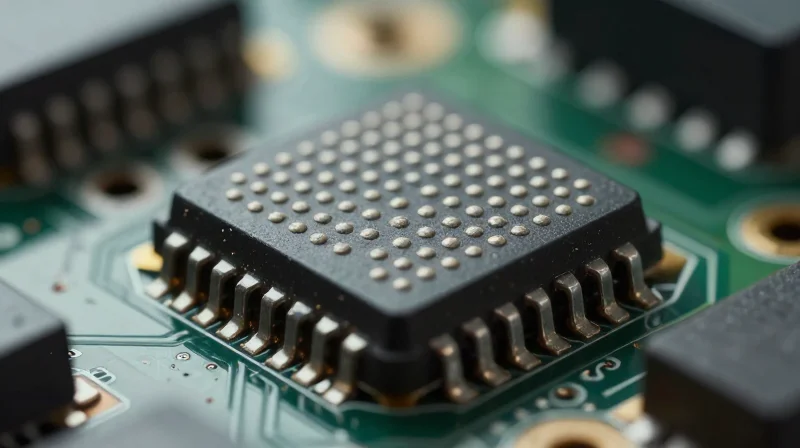
The Nature of BGA Interconnect Complexity
Unlike standard surface-mount devices where solder joints are peripheral and visually inspectable, BGA components conceal their interconnects beneath the package body. This architectural shift means that physical inspection via conventional optical systems is ineffective, placing the burden of quality control entirely on robust design for manufacturing (DFM) guidelines and precise process engineering.
Key Variables Influencing Assembly Success
| Variable | BGA Impact | Assembly Risk |
|---|---|---|
| Thermal Mass | High density causes uneven heating | Head-in-pillow or cold joints |
| Solder Paste Volume | Tiny apertures require precision | Insufficient volume or bridging |
| Coplanarity | Package warpage during reflow | Open circuits on outer pins |
Common Assembly Pitfalls and Risks
The primary risk in BGA assembly is the formation of latent defects that may pass electrical testing but fail prematurely in the field. Issues such as voiding within the solder spheres or inconsistent wetting are common when thermal profiles do not account for the specific thermal mass of the BGA component.
- Why are BGA solder joints harder to inspect?
Because the joints are located underneath the chip, they are physically inaccessible to standard inspection cameras, requiring X-ray (AXI) or CT scanning. - What is the primary cause of BGA solder failure?
Thermal stress during reflow and mechanical stress post-assembly are the leading causes, often exacerbated by CTE (Coefficient of Thermal Expansion) mismatches between the PCB and the component. - How does PCB design affect BGA yield?
Via-in-pad strategies, trace routing density, and copper balance significantly impact heat distribution and solder paste stencil printing consistency.
The Foundation: Pad Sizing and Solder Mask Design
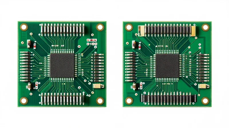
NSMD vs. SMD: Defining the Pad Geometry
The primary decision in BGA land pattern design is choosing between Non-Solder Mask Defined (NSMD) and Solder Mask Defined (SMD) pads. NSMD pads are defined by the copper etching process, where the solder mask opening is larger than the copper pad, allowing the solder to wrap around the sides of the pad. Conversely, SMD pads are defined by the solder mask opening being smaller than the copper pad, with the mask covering the edges of the copper.
| Feature | NSMD (Non-Solder Mask Defined) | SMD (Solder Mask Defined) |
|---|---|---|
| Copper Pad Area | Smaller than mask opening | Larger than mask opening |
| Solder Joint Strength | Superior (side wetting) | Lower (less surface area) |
| Registration Risk | Higher reliance on etching | Higher reliance on mask alignment |
| Best Application | Fine pitch, high reliability | Dense boards, via-in-pad |
Impact on Solder Joint Reliability
The choice between these designs directly dictates how a joint handles mechanical and thermal stress. NSMD pads provide a larger surface area for the solder, creating a 'wraparound' effect that enhances mechanical interlocking. While this improves fatigue resistance during thermal expansion cycles, it requires tighter tolerances in the PCB manufacturing process. SMD pads are often employed to prevent solder wicking into nearby vias, but they are more prone to lifting from the laminate under extreme stress because the mask effectively 'chokes' the fillet formation.
Key Considerations for Pad Design
- Why is NSMD generally preferred for BGAs?
NSMD provides better long-term fatigue resistance due to increased solder fillet area around the copper pad edges, which is critical for mitigating stress during thermal cycling. - When is it necessary to use SMD?
SMD is often required for high-density designs where microvias must be placed directly in or adjacent to the pad to prevent solder from wicking away into the hole. - How does solder mask clearance affect assembly?
Improper clearance can lead to 'mask encroachment,' where the mask touches the pad, creating an uneven surface that forces the BGA ball to sit off-center, leading to common bridging or open-circuit defects.
Designers should maintain a minimum solder mask clearance of 0.05mm to 0.075mm for NSMD designs to ensure that the mask does not interfere with the solder joint. Always consult your fabricator for their specific registration capabilities, as these tolerances define the success of high-density interconnect designs.
Stencil Engineering for Consistent Volume Control
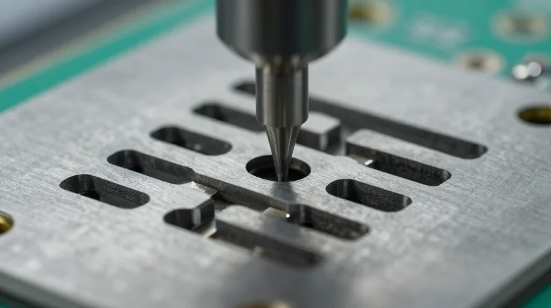
Precision stencil engineering acts as the primary gatekeeper for solder volume consistency in BGA assembly. By balancing stencil thickness with carefully calibrated aperture dimensions, manufacturers can achieve the ideal solder transfer efficiency required for high-density ball grid arrays, effectively mitigating risks associated with both solder starvation and excess bridging.
Optimizing Stencil Parameters for Fine-Pitch BGAs
The relationship between stencil thickness and aperture area ratio is critical to successful paste release. For fine-pitch BGAs, an area ratio greater than 0.66 is typically required to ensure adequate solder transfer. Failure to respect these ratios leads to intermittent connection issues caused by insufficient volume.
| Parameter | Standard Practice | Design Consideration |
|---|---|---|
| Stencil Thickness | 0.10mm - 0.15mm | Thinner foils improve release for fine-pitch. |
| Aperture Shape | Rounded Rectangle | Reduces paste adhesion to walls. |
| Area Ratio | > 0.66 | Critical for high-density transfer efficiency. |
Material Selection and Aperture Design
Modern BGA assemblies demand advanced stencil materials. Laser-cut stainless steel with electro-polished apertures is the industry standard for maintaining consistent volume. For ultra-fine pitch components, nano-coating the stencil surface is a recommended strategy to drastically improve paste release and reduce the frequency of manual stencil wiping cycles.
- How does aperture geometry affect paste release?
Apertures with rounded corners or tapered walls reduce friction during the printing process, ensuring a cleaner release and consistent transfer of paste onto the PCB pads. - Why is stencil thickness a common failure point?
Excessive thickness can lead to solder bridging on fine-pitch components, while overly thin stencils lead to insufficient solder joints, causing mechanical failure during thermal cycling. - When should nano-coatings be implemented?
Nano-coatings should be prioritized whenever the BGA pitch drops below 0.5mm, as this dramatically improves transfer efficiency and prevents the paste from clogging the aperture walls.
Strategic Trace Routing and Via-in-Pad Techniques
As BGA pitch requirements tighten, routing signals out of the package footprint becomes a significant manufacturing challenge. Effective BGA routing requires a balanced approach between signal integrity and thermal-mechanical reliability. Improper trace attachment to pads acts as a thermal heat sink or a conduit for solder wicking, both of which are primary contributors to open circuits and cold solder joints during reflow.
Mitigating Solder Wicking Risks
Solder wicking occurs when molten solder flows away from the BGA ball through exposed copper traces or unsecured vias, depriving the joint of necessary volume. To mitigate this, engineers must enforce specific layout rules for signal breakout.
- Trace Necking
Always taper traces to a narrower width before they reach the BGA pad. This high-resistance thermal path prevents the trace from acting as a heat sink during the soldering process. - Solder Mask Dam (Webs)
Maintain a minimum of 75-100μm of solder mask between pads. This dam prevents bridge-inducing solder flow and acts as a barrier to keep paste contained on the pad surface. - Via Placement
Avoid placing vias directly adjacent to pads without an intervening mask dam, as this provides a direct path for solder to wick into the barrel.
Via-in-Pad (VIPPO) Best Practices
For fine-pitch components where traditional dog-bone routing is impossible, Via-in-Pad Plated Over (VIPPO) is the industry standard. However, failure to process these correctly leads to catastrophic voiding or pin-hole defects.
| Feature | Requirement | Purpose |
|---|---|---|
| Plating | Copper Capped | Creates a flat, solderable surface. |
| Planarity | < 12μm | Ensures consistent paste deposition. |
| Drill Size | 0.10mm - 0.15mm | Optimizes via density vs. mechanical integrity. |
Common Routing FAQs
- Why must I use VIPPO over standard dog-bone routing for 0.5mm pitch BGAs?
0.5mm pitch does not provide enough physical space to run a trace between pads while maintaining standard trace-to-copper clearances, making VIPPO essential for density. - How does via-in-pad affect solder volume?
If a via is not fully filled and capped (planarized), solder will wick into the via hole during reflow, leading to insufficient solder at the joint and potential open circuits.
Conquering Head-in-Pillow (HiP) Defects

Understanding the Mechanics of HiP Defects
Head-in-Pillow occurs when the BGA solder ball and the printed solder paste do not achieve full wetting during the reflow process. This is typically caused by package warpage during thermal cycling, where the ball lifts away from the paste just as the flux becomes active, creating a non-coalesced electrical contact that is notoriously difficult to detect via standard Automated Optical Inspection (AOI).
DFM Strategies for Mitigating HiP
- Stencil Aperture Geometry
Utilize home-plate or rounded-corner apertures to increase the volume of paste deposited, ensuring the paste maintains contact with the BGA ball even if the package warps during the liquidus phase. - Reflow Profile Optimization
Extend the soak time and ensure the temperature delta across the assembly is minimized. A longer soak allows the package and the PCB to reach thermal equilibrium, reducing the magnitude of warpage. - Solder Paste Selection
Specify Type 4 or Type 5 solder pastes with high-activity flux chemistries, which are engineered to resist oxidation and maintain wetting properties over broader thermal windows.
Comparison of Mitigation Techniques
| Strategy | Primary Benefit | DFM Implementation Complexity |
|---|---|---|
| Aperture Optimization | Increases paste-to-ball engagement | Low |
| Profile Modification | Reduces dynamic warpage | Medium |
| Paste Chemistry | Enhances flux wetting capacity | Low |
Frequently Asked Questions
- Can X-Ray verify HiP defects?
Standard 2D X-Ray often fails to detect HiP. 3D X-Ray or Computed Tomography (CT) is required to identify the gap between the ball and the pad accurately. - Why does package warpage occur?
Warpage is induced by the Coefficient of Thermal Expansion (CTE) mismatch between the silicon die, the molding compound, and the substrate materials within the BGA package.
Reflow Profile Optimization for BGA Reliability
Achieving a robust solder joint for high-pin-count BGAs relies on the synchronization of thermal mass across the component footprint. A non-uniform reflow profile often leads to thermal gradients, causing the center of the BGA to lag behind the perimeter, which induces stress and potential open circuits. Proper profiling necessitates a balance between flux activation time and the liquidus duration, ensuring that all solder balls reach a state of complete coalescence without compromising component integrity.
The Role of the Soak Zone in BGA Reliability
The soak zone is critical for stabilizing temperatures across varying component masses. If the soak duration is too short, the flux fails to effectively clear oxides, leading to poor wetting. Conversely, an excessively long soak can exhaust the flux prematurely, resulting in head-in-pillow (HiP) defects. For high-density arrays, the soak should be optimized to reach a thermal equilibrium, allowing the temperature differential between the BGA body and the PCB substrate to minimize before transitioning into the spike.
| Parameter | Recommended Range | Impact of Improper Setting |
|---|---|---|
| Soak Duration | 60–120 seconds | Short: Voids/Cold Joints; Long: Flux exhaustion/HiP |
| Soak Temperature | 150°C–180°C | Low: Incomplete wetting; High: Premature oxidation |
| Time Above Liquidus (TAL) | 45–90 seconds | Low: Weak IMC; High: Excessive intermetallic layer |
Reflow Optimization FAQs
- How does PCB thickness influence BGA reflow?
Thicker PCBs have higher thermal mass, acting as a heat sink that can delay the BGA center from reaching liquidus. This requires a longer soak period to ensure the substrate matches the component temperature. - What is the consequence of reaching too high a peak temperature?
Excessive peak temperature can cause component warping, damage to internal sensitive substrates, and brittle intermetallic compound (IMC) formation, which drastically reduces the fatigue life of the solder joint. - Can nitrogen reflow improve BGA yields?
Yes, using a nitrogen (N2) atmosphere broadens the processing window by suppressing oxidation, which is particularly beneficial for complex BGAs with fine-pitch or lead-free alloys prone to surface contamination.
Mitigating Solder Bridging in High-Density Layouts
Solder bridging in high-density BGA layouts often occurs when excessive solder volume or poor registration causes adjacent balls to coalesce during the liquidus stage. As component pitches shrink below 0.5mm, the margin for error diminishes significantly, requiring a shift toward Solder Mask Defined (SMD) pad architectures and highly controlled stencil deposition parameters to maintain electrical isolation.
Critical Layout Strategies for Bridging Prevention
- Solder Mask Defined (SMD) vs. Non-SMD
Utilize SMD pads for fine-pitch BGAs. By partially covering the copper pad with solder mask, you create a physical barrier that constrains the solder paste, providing better registration and preventing the molten solder from leaching into adjacent channels. - Stencil Aperture Reduction
Implement a 10% to 15% area reduction in stencil apertures compared to pad dimensions. This ensures sufficient solder volume for a reliable joint while mitigating the risk of excess paste squeezing out into the bridging-prone inter-pad gap. - Optimizing Trace Routing
Avoid routing high-speed traces directly between BGA pads unless absolutely necessary. If required, ensure the solder mask web between pads remains at least 0.1mm wide to prevent potential shorts during the liquidus state.
Comparison of Pad Design Techniques
| Feature | Non-SMD (NSMD) | SMD (Solder Mask Defined) |
|---|---|---|
| Registration | Depends on PCB etching | Controlled by solder mask process |
| Bridging Risk | Higher due to exposed copper | Lower due to mask barrier |
| Mechanical Strength | Higher fatigue resistance | Slightly lower at mask interface |
Frequently Asked Questions
- How does stencil thickness affect bridging?
Thicker stencils increase the volume of deposited paste. For high-density BGAs, using a thinner stencil (e.g., 0.1mm vs 0.12mm) can drastically reduce bridging by limiting the paste volume per pad. - Can solder mask web width be too small?
Yes. If the web width is below the manufacturing capability (typically < 0.1mm), the mask may break or lift during reflow, leading to unpredictable solder pooling and bridge formation.
Inspection and Testing Protocols

X-Ray Inspection for Hidden Solder Joints
Because BGA components feature solder balls hidden beneath the package body, standard Automated Optical Inspection (AOI) is insufficient. 2D and 3D Automated X-Ray Inspection (AXI) systems are mandatory to evaluate internal structural integrity. These systems identify critical failures such as voids, bridging, and insufficient solder volume that occur due to improper wetting or reflow imbalances.
| Defect Type | Detection Capability | Risk Level |
|---|---|---|
| Solder Voids | High (AXI) | Medium |
| Bridging | High (AXI) | Critical |
| Head-in-Pillow | Medium (3D AXI) | Critical |
| Insufficient Solder | High (2D/3D AXI) | High |
Validating Long-term Reliability via Thermal Cycling
While X-ray confirms initial assembly quality, thermal cycling tests validate the long-term structural reliability of BGA solder joints. By exposing the PCB to alternating temperature extremes, we simulate field operational stress, revealing potential weaknesses in material compatibility and Coefficient of Thermal Expansion (CTE) mismatches.
- Why is 3D AXI preferred over 2D for high-density BGAs?
3D AXI (Computed Tomography) provides cross-sectional views, enabling the inspection of multiple layers and identifying defects that 2D X-ray obscures, such as hidden shorts or internal ball-to-pad separation. - How many thermal cycles are standard for BGA verification?
While requirements vary by industry (e.g., IPC-9701), standard reliability testing typically ranges from 500 to 1,000 cycles, depending on the service environment and the desired lifespan of the electronic assembly. - What indicates a failure during thermal cycling?
Failure is typically indicated by an increase in resistance or an intermittent open circuit within the daisy-chained BGA network, signifying the propagation of micro-cracks in the solder intermetallic layer.
By adhering to these rigorous DFM standards, you can transform your BGA assembly process from a potential failure point into a hallmark of reliability. Precision in design and process control is the key to minimizing rework and accelerating time-to-market. Contact our engineering team today to review your current board layout and ensure your next project meets the highest industry standards.
