
Reliability is the heartbeat of every CNC machine. When designing high-speed control logic, even minor oversights in DFM can lead to signal degradation or catastrophic thermal failure. This guide breaks down the mission-critical design standards required to move your prototype into high-yield, industrial-grade production.
The Critical Role of DFM in CNC Systems
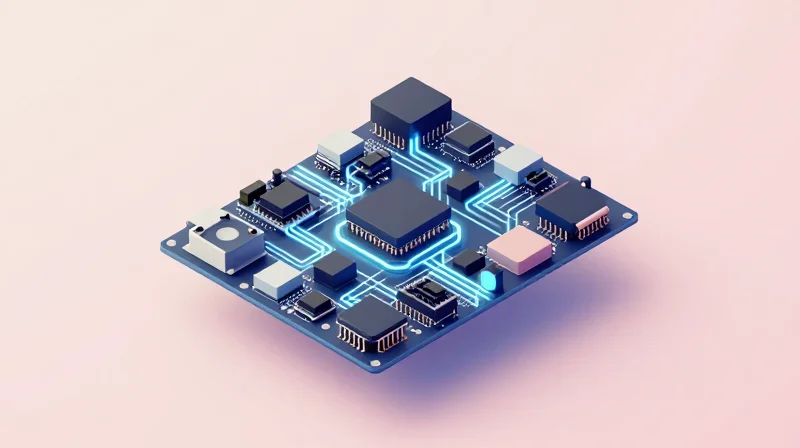
Why DFM Dictates CNC Board Reliability
In the context of CNC control boards, DFM is not merely a cost-reduction strategy; it is a critical engineering discipline that directly dictates the longevity and accuracy of the motion control loop. Because CNC controllers operate in electrically noisy environments with high-speed PWM signals, poor layout decisions—such as improper trace routing or inadequate thermal management—can introduce jitter, electromagnetic interference (EMI), and premature component degradation.
Strategic Advantages of Early DFM Integration
- Prevention of Signal Integrity Issues
Early DFM analysis identifies potential crosstalk and impedance mismatches before physical prototyping, ensuring high-speed signals remain clean under load. - Optimizing Thermal Dissipation
Proper copper weight and heat-sinking placement facilitate the thermal management necessary for boards driving high-torque stepper or servo motor interfaces. - Reducing Assembly Errors
Adhering to standard component footprints and spacing guidelines minimizes SMT placement errors, which is critical for boards packed with precision microcontrollers.
| Design Phase | DFM Impact | Outcome |
|---|---|---|
| Conceptual | Component Selection | Lower BOM cost and better supply chain resilience |
| Layout | Trace/Plane Routing | Reduced noise floor and improved EMI performance |
| Pre-Production | DFA Validation | Elimination of assembly reworks and scrap |
DFM Checklist for High-Precision CNC Designs
Engineers should prioritize specific manufacturing constraints during the CAD phase to ensure the board meets the stringent requirements of machine tool controllers. This includes defining minimum trace widths, maintaining optimal via-to-pad clearances, and ensuring that silk-screen identifiers do not overlap critical solder masks. By standardizing these parameters early, manufacturers can achieve consistent signal integrity across batches, effectively insulating the control system against field failures in harsh industrial workshops.
Precision Impedance Control for High-Speed Signals

Engineering Precision Impedance Control
For CNC control boards, maintaining consistent impedance is non-negotiable for high-speed differential signals, such as LVDS or high-speed encoder feedback. Signal reflections, caused by impedance discontinuities, directly translate to jitter and communication errors that jeopardize motion precision. Achieving a target impedance, typically 50Ω single-ended or 100Ω differential, requires a rigorous synergy between trace geometry, dielectric constant consistency, and precise manufacturing stack-up tolerances.
Material Selection and Stack-Up Geometry
The foundation of impedance control is the dielectric constant (Dk) of the PCB laminate. To maintain stable impedance across varying environmental conditions often found in CNC enclosures, utilize FR-4 variants with a tightly controlled Dk tolerance. Designers must work with manufacturers to specify a balanced layer stack-up, ensuring that high-speed layers are referenced to continuous ground planes, avoiding split planes that force current to return through high-inductance paths.
| Parameter | Control Priority | Impact on Impedance |
|---|---|---|
| Trace Width | High | Inversely proportional |
| Dielectric Thickness | High | Directly proportional |
| Copper Thickness | Medium | Inverse effect (fringing) |
| Dielectric Constant (Dk) | High | Inversely proportional |
Frequently Asked Questions on Impedance Design
- How do copper etching tolerances affect impedance?
Etching variations cause the actual trace width to deviate from the design value. A standard tolerance of ±10% on trace width can lead to a 3-5% variance in impedance, necessitating strict manufacturing cooperation. - Why must high-speed signals avoid plane splits?
Impedance relies on the return path directly beneath the signal trace. Crossing a split plane introduces an abrupt change in the return path geometry, creating an inductive discontinuity and increasing EMI. - Should I rely on software calculators or manufacturer data?
While software tools provide a theoretical baseline, always use the specific Dk and resin content data provided by your PCB manufacturer to ensure the calculation aligns with their production capabilities.
Strategic Component Placement for EMI Mitigation
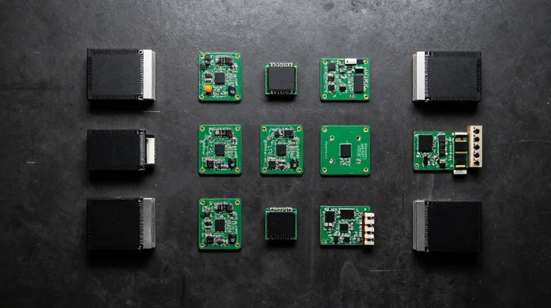
In high-precision CNC control boards, the coexistence of high-current switching regulators and microvolt-level analog feedback sensors creates a significant risk for electromagnetic interference (EMI). Effective DFM strategies prioritize the physical partitioning of the PCB, ensuring that high-frequency return currents do not intersect with sensitive signal paths, thereby maintaining signal integrity and motion accuracy.
Zonal Partitioning Methodology
The most robust defense against EMI is strict zonal partitioning. By establishing physical 'keep-out' zones, designers can effectively isolate noisy power stages from the sensitive feedback loops responsible for motor positioning data. Components should be grouped by their functional classification and noise signature.
| Circuit Zone | Interference Profile | Design Strategy |
|---|---|---|
| Power/Switching | High dV/dt, High di/dt | Isolate to edge, minimize loop area |
| Digital Logic | High-speed clock noise | Use internal ground planes |
| Analog Feedback | Ultra-sensitive to jitter | Differential pairs, remote ground sensing |
Common Questions on Component Isolation
- How far should switching regulators be placed from analog input stages?
As a general DFM rule, aim for a minimum of 20-30mm of separation. If space is constrained, implement a continuous ground plane with a dedicated split or a guard trace tied to chassis ground to block direct coupling. - Does the orientation of inductors impact EMI?
Yes, inductors should be placed with their magnetic field axes oriented perpendicularly to sensitive trace runs. Avoid grouping multiple power inductors parallel to one another to prevent inductive crosstalk.
Ground Plane Integrity
The ground plane is not just a return path; it is an EMI shield. To minimize noise injection, ensure that the return path for high-speed switching regulators is tightly constrained underneath the top layer power traces, preventing high-frequency loops from expanding across the entire board surface. For precision CNC feedback, utilize a 'Star Ground' topology near the ADC (Analog-to-Digital Converter) to ensure that the reference ground remains pristine despite the presence of high-current power stages.
Advanced Thermal Management Techniques
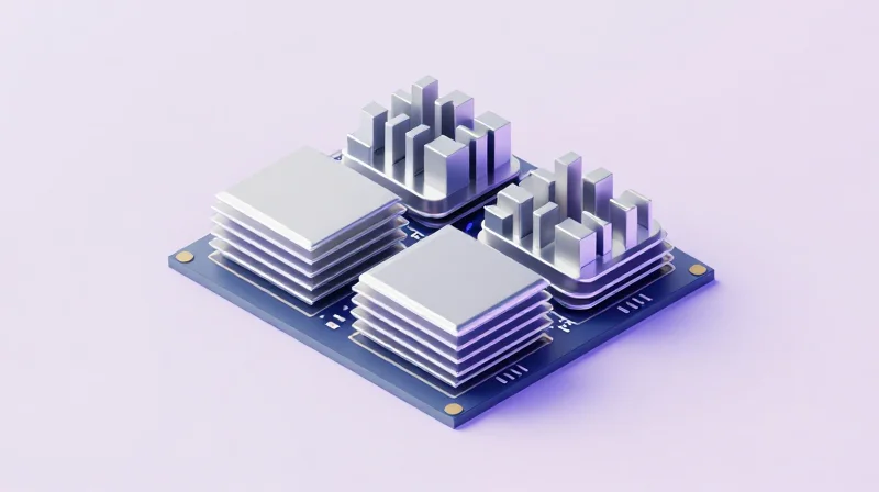
Integrated Thermal Dissipation Strategies
In high-precision CNC controllers, space constraints often preclude traditional airflow, necessitating board-level thermal management. By leveraging thermal vias as low-resistance paths to inner ground planes, designers can transform the entire PCB into a high-capacity heat sink, effectively drawing energy away from sensitive components like MOSFETs and high-speed processors.
Thermal Management Comparison
| Technique | Primary Application | Efficiency Level |
|---|---|---|
| Thermal Vias | High-density ICs / Power stages | High |
| Heavy Copper Pours | Global board cooling | Medium |
| Active Heatsinks | High-TDP Processors | Very High |
| Thermal Interface Materials | Gap filling to chassis | High |
Best Practices for Implementation
- How should thermal vias be arrayed?
Thermal vias should be arranged in a tightly packed grid directly under the component's exposed thermal pad, utilizing a pitch of 0.8mm to 1.0mm to maximize copper cross-sectional area without violating manufacturing drill-density constraints. - Why prioritize copper pour thickness?
Increasing the outer layer copper weight to 2oz allows for lower thermal resistance spreading, which is crucial when the CNC controller is mounted directly to a metal heat-dissipating chassis. - How can I bridge the gap to the enclosure?
Utilize thermally conductive gap pads that bridge the distance between top-side hot components and the aluminum controller housing, effectively turning the entire CNC enclosure into a passive radiator.
Design for Manufacturing (DFM) Considerations
When incorporating these techniques, ensure that thermal vias are tented or plugged with epoxy to prevent solder wicking during the reflow process, which can lead to voids and unreliable thermal junctions. Furthermore, avoid placing components requiring thermal relief in areas of high-vibration typical of CNC environments, as concentrated heat can accelerate solder joint fatigue. Always simulate thermal profiles during the design phase to identify 'hot spots' before committing to high-volume manufacturing.
Optimizing Layer Stack-up for Power Integrity
Achieving stable power delivery in high-precision CNC controllers requires a rigorous approach to stack-up design. By prioritizing low-impedance power distribution networks (PDN) and maximizing inter-plane capacitance, designers can effectively mitigate ground bounce and transient supply noise, ensuring the consistent voltage levels critical for high-speed processor reliability.
Core Principles of Power Integrity Stack-up
- Prioritize Plane Coupling
Place power and ground planes on adjacent layers with the thinnest possible dielectric. This maximizes inter-plane capacitance, which acts as a high-frequency filter for power distribution. - Maintain Ground Plane Continuity
Ensure solid, uninterrupted ground planes beneath high-speed signals and power planes. Avoiding splits or voids in ground references prevents return path inductance spikes. - Symmetry and Balance
Utilize a symmetrical stack-up to prevent board warping during reflow, which is essential for maintaining consistent dielectric thickness and impedance control across the board.
Comparison of Stack-up Strategies
| Strategy | Power Integrity Benefit | Design Trade-off |
|---|---|---|
| Tight Plane Coupling | Reduces high-frequency noise | Increases manufacturing complexity |
| Distributed Decoupling | Lower loop inductance | Requires higher via density |
| Dedicated Ground Layers | Minimizes EMI and return noise | Increases layer count and cost |
Mitigating High-Frequency Noise
To effectively combat switching noise, implement a multi-tiered decoupling strategy. Ensure that decoupling capacitors are placed as close as possible to the IC power pins, utilizing short, wide traces or multiple vias to minimize mounting inductance. Furthermore, integrate a solid reference plane structure that provides low-inductance return paths, effectively dampening electromagnetic emissions and preserving signal integrity across the CNC control logic.
Via Design and Drill Standards for Industrial Yield
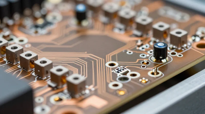
The Engineering Balance: Via Aspect Ratios
In high-precision CNC control boards, the via aspect ratio—defined as the ratio of board thickness to drill diameter—is a critical determinant of plating quality. A higher aspect ratio increases the difficulty for plating solutions to reach the center of the via barrel, often resulting in cracked barrels or intermittent conductivity under thermal stress. Standard DFM practices dictate maintaining an aspect ratio of 10:1 or lower for high-volume production, though specialized fabricators may accommodate up to 12:1 with advanced pulse plating techniques.
| Via Type | Recommended Aspect Ratio | Design Consideration |
|---|---|---|
| Standard Thru-hole | 8:1 | Cost-effective, standard drills |
| High-Density Thru-hole | 10:1 | Requires strict plating controls |
| Micro-via (Laser) | 0.75:1 | Must be capped with copper |
Strategic Via-in-Pad Implementation
Via-in-pad (VIPPO) is essential for escaping high-pin-count BGA packages in dense CNC controllers, but it introduces significant manufacturing risks if not properly prepared. To prevent solder wicking and potential voiding, via holes must be filled with a conductive or non-conductive epoxy and subsequently planarized with a copper cap. This creates a solid, conductive surface for component mounting, preventing solder paste migration during reflow.
- Why is copper capping mandatory for via-in-pad?
Without a copper cap, the solder paste would be drawn into the via hole during reflow, leading to joint starvation and fragile electrical connections. - How does via size impact drill wander?
Smaller drill diameters are prone to deflection during the drilling process; therefore, aggressive drill tolerances require thicker annular rings to ensure the hole lands accurately within the capture pad. - What is the primary risk of exceeding aspect ratio limits?
Exceeding recommended ratios causes 'plating starvation,' where the copper deposit is too thin in the center of the hole, leading to board failure during thermal cycling or vibration.
Prototyping Recommendation
# Example Design Constraint Check
DRC_ASPECT_RATIO_MAX = 10
def validate_via(thickness, drill_diameter):
    if (thickness / drill_diameter) > DRC_ASPECT_RATIO_MAX:
        return "FAIL: Exceeds fabrication capability"
    return "PASS"
Silkscreen and Assembly Considerations
Silkscreen clarity and solder mask accuracy are critical determinants of assembly throughput and long-term diagnostic reliability in industrial CNC environments. By aligning silkscreen labels with automated optical inspection (AOI) requirements and defining proper solder mask openings, designers can drastically reduce manual rework and installation errors.
Best Practices for Silkscreen Legibility and Placement
Silkscreen should serve as a functional roadmap for field technicians and assembly machines. Avoid placing markings over test points, copper pads, or areas prone to high thermal stress, as these can cause flaking or obscure critical board information.
- Maintain Minimum Clearance
Keep silkscreen at least 0.1mm (4 mils) away from exposed copper to prevent registration issues during the printing process. - Standardized Font Sizing
Use a minimum stroke width of 0.15mm (6 mils) and a height of at least 1mm (40 mils) to ensure readability after reflow. - Reference Designator Alignment
Consistently orient designators in the same direction for all components to simplify manual inspection and board troubleshooting.
Solder Mask Relief and Manufacturing Yield
Inadequate solder mask relief can lead to tombstoning or unintended solder bridges, especially on high-density CNC controller boards. Standardizing your expansion settings ensures reliable surface mount technology (SMT) results.
| Feature Type | Recommended Expansion | Rationale |
|---|---|---|
| Standard SMT Pads | 0.05mm - 0.075mm | Prevents solder mask encroachment on pads. |
| Fine Pitch ICs | 0.025mm - 0.05mm | Prevents bridging between tight leads. |
| Vias (Tented) | None (Negative Expansion) | Protects vias from shorting during wave soldering. |
Assembly-Centric Design Considerations
To maximize throughput on automated assembly lines, designers must incorporate fiducials and ensure symmetrical thermal distribution across solder pads. Fiducials should be placed on at least three corners of the board to provide the machine with accurate global positioning data, minimizing the risk of misaligned components during high-speed pick-and-place operations.
Verification: Testing for Industrial Compliance
Comprehensive Verification Strategies
For high-precision CNC controllers, verification transcends standard continuity testing. Designers must implement rigorous validation methods to ensure signal integrity, thermal stability, and long-term industrial compliance in high-vibration, electrically noisy environments.
Validation Methodologies
| Method | Primary Goal | Industrial Metric |
|---|---|---|
| TDR Measurement | Impedance Profile | Controlled 50/100 Ohm tolerance |
| Thermal Imaging | Hotspot Detection | Component T-rise limits |
| Flying Probe | Short/Open Detection | Netlist fidelity |
| Vibration Stress | Solder Joint Integrity | MIL-STD-810H compliance |
FAQ: Validating Industrial Compliance
- Why is TDR critical for CNC boards?
Time Domain Reflectometry (TDR) is essential for validating trace impedance, which prevents signal reflections that could lead to erratic motion control or encoder data corruption. - How does thermal imaging improve reliability?
Thermal mapping reveals parasitic power dissipation in high-speed switching circuits, allowing for layout adjustments before production to prevent localized component aging. - What defines compliance for EMI/EMC?
Industrial compliance requires meeting IEC 61000 standards, validated through radiated emissions testing and susceptibility checks to ensure the control board functions in proximity to high-current motors.
Prototyping Best Practices
Always maintain a 'golden sample' for comparison during the transition from prototype to mass production. Automated Optical Inspection (AOI) should be calibrated against this sample to ensure consistent verification of solder fillets and component placement throughout the manufacturing life cycle.
By adhering to these DFM best practices, you can ensure your CNC control boards withstand the demands of intense industrial environments. Ready to take your design to the next level? Contact our expert engineering team today for a comprehensive DFM audit of your next project.
