
As data center speeds accelerate to 400G and 800G, the margin for error in PCB design has vanished. Engineers face an unprecedented challenge: balancing aggressive manufacturing constraints with the unforgiving physics of high-frequency signal propagation. In this guide, we break down the critical DFM rules and signal integrity strategies required to build next-generation switch hardware that performs reliably under extreme bandwidth demands.
The Physics of High-Speed Interconnects

The 28GHz Threshold: Why Physics Matters
As data rates scale toward 112Gbps PAM4 and beyond, signal integrity challenges evolve from simple trace impedance mismatches into complex electromagnetic interactions. At frequencies exceeding 28GHz, the dielectric constant (Dk) and dissipation factor (Df) of PCB materials become critical, as the skin effect and surface roughness dominate signal attenuation, turning PCB traces into significant low-pass filters.
Key Degradation Mechanisms
| Phenomenon | Physical Cause | Impact on Signal |
|---|---|---|
| Skin Effect | Current crowding at trace surface | Increased AC resistance |
| Fiber Weave Effect | Non-uniform glass distribution | Skew and timing jitter |
| Dielectric Loss | Molecular polarization of resin | Amplitude attenuation |
| Surface Roughness | Copper foil irregularities | Phase shift and EMI |
Practical FAQs on High-Speed Physics
- How does copper foil roughness affect insertion loss?
As frequency increases, current is forced into the microscopic 'valleys' of the copper surface. This increases the effective path length and resistance, leading to significant signal attenuation. - What is the primary cause of intra-pair skew in high-frequency designs?
The fiber weave effect, where differential signals propagate over different glass or resin regions, creates variations in effective Dk, causing phase mismatch. - Why is 28GHz considered a critical design inflection point?
Beyond 28GHz, traditional PCB design assumptions regarding lumped-element circuit models fail, necessitating full-wave 3D electromagnetic field simulation to predict performance accurately.
Precision Stack-Up Design for Minimal Loss
Selecting Dielectrics for 28GHz+ Applications
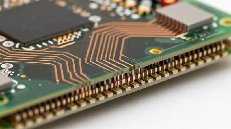
At frequencies exceeding 28GHz, the dielectric constant (Dk) and dissipation factor (Df) of your laminate are critical determinants of signal throughput. To minimize insertion loss, designers must prioritize materials with a stable Dk across a broad frequency spectrum and ultra-low Df values, typically below 0.002.
| Material Category | Target Df (@ 28GHz) | Primary Application |
|---|---|---|
| PTFE/Ceramic | < 0.001 | Ultra-high-speed backplanes |
| Modified Epoxy | 0.0015 - 0.002 | Mainboard signal routing |
| Standard FR4 | > 0.010 | Not recommended for >10Gbps |
Mitigating Skin Effect via Surface Roughness Optimization
As signal frequency rises, the skin effect restricts electron flow to the outer surface of the copper trace. If the copper foil is too rough, the effective path length increases significantly, leading to higher ohmic losses. Utilizing VLP (Very Low Profile) or HVLP (Hyper Very Low Profile) copper is mandatory to ensure the surface profile remains well below the skin depth at operational frequencies.
Design Best Practices for Stack-Up Integrity
- How does copper roughness affect high-frequency loss?
Increased roughness increases the effective path length for high-frequency signals, exacerbating the skin effect and leading to significant conductor loss. - What is the role of glass weave effect?
The heterogeneous nature of glass fibers in standard prepreg causes Dk variations; using spread-glass or non-woven laminates is essential to maintain signal timing skew within acceptable tolerances. - Should I prioritize Dk or Df?
While Dk stability is vital for impedance control, Df is the dominant driver of attenuation. Always target the lowest available Df for the specific frequency band required.
Advanced Impedance Control Strategies
Advanced Impedance Control Strategies
In switch fabrics operating at 56G/112G PAM4, maintaining a tight impedance tolerance (typically ±5%) is no longer optional. Beyond standard stack-up planning, engineers must employ dynamic manufacturing compensation techniques. This includes adjusting CAD artwork for etch-back effects, accounting for the variation in dielectric constant (Dk) across glass weave patterns, and implementing localized reference plane management to mitigate discontinuities at via transitions.
Strategies for Maintaining Uniformity
- Fiber Weave Effect Mitigation
Utilize spread glass fabrics or rotate PCB traces at an angle (typically 10-15 degrees) relative to the weave to average out local Dk variations, preventing intra-pair skew and impedance ripples. - Etch Compensation Profiles
Collaborate with fabricators to apply non-linear etch compensation factors based on trace density and layer-specific copper weight to ensure the final geometry matches the design simulation. - Via Stubs and Back-Drilling
To maintain signal integrity, eliminate resonant via stubs through high-precision back-drilling, which drastically reduces parasitic capacitance and improves TDR performance at high frequencies.
| Control Method | Primary Benefit | Design Consideration |
|---|---|---|
| Zig-Zag Routing | Reduces fiber weave impact | Increases total trace length |
| Back-drilling | Improves Return Loss | Requires strict drill depth tolerance |
| Ground Stitching | Provides continuous return path | Must balance with density limits |
By integrating these advanced control strategies, design teams can stabilize impedance across the high-speed signal path, ensuring robust performance for the next generation of data center switching architectures.
Mitigating Crosstalk in High-Density Layouts
As signaling speeds push beyond 56Gbps and 112Gbps PAM4, the proximity of traces in high-density switch fabrics creates significant electromagnetic coupling. Mitigating this crosstalk is not merely about physical separation; it involves precise control over reference plane continuity and the reduction of field leakage through aggressive impedance management.
Advanced Coupling Management Strategies
The fundamental defense against crosstalk is the management of the return path. By ensuring that signal traces are tightly coupled to their respective reference planes, designers minimize the loop area through which magnetic flux can radiate. For differential pairs, the focus must shift to maintaining symmetric coupling, as any imbalance results in mode conversion and increased EMI.
| Mitigation Strategy | Primary Mechanism | Recommended Practice |
|---|---|---|
| Trace Separation | Distance-based isolation | 3H to 5H rule (H=dielectric height) |
| Reference Stitching | Return path continuity | Add ground vias near signal vias |
| Layer Assignment | Field containment | Use stripline over microstrip |
Best Practices for Layer Transitioning
Every layer transition presents an impedance discontinuity. To minimize crosstalk during these transitions, signal vias must be accompanied by dedicated ground stitching vias. This practice ensures that the return current has an uninterrupted path, preventing localized current crowding that often acts as a source for capacitive crosstalk between adjacent via barrels.
Frequently Asked Questions
- Why is stripline preferred over microstrip for high-speed routing?
Stripline provides superior EMI shielding because the signal layer is sandwiched between two reference planes, significantly reducing the leakage of electromagnetic fields into neighboring traces. - How many ground stitching vias are required per signal transition?
While a 1:1 ratio is ideal for 112Gbps architectures, a minimum of two stitching vias per signal pair is recommended to ensure low-inductance return path management. - Does copper surface roughness impact crosstalk?
Yes. Higher roughness increases dielectric loss and localized impedance variations, which can inadvertently create reflections that complicate the crosstalk budget within the channel.
Essential DFM Rules for High-Frequency PCBs
Optimizing Drill and Via Reliability
At frequencies exceeding 28GHz, the physical geometry of vias significantly impacts both signal integrity and manufacturing success. Establishing strict drill-to-copper clearances is essential to prevent shorts, while maintaining optimal aspect ratios ensures reliable plating in high-layer-count backplanes.
| Parameter | Recommended Threshold | Impact |
|---|---|---|
| Max Aspect Ratio | 10:1 to 12:1 | Ensures uniform copper deposition |
| Drill-to-Copper Clearance | > 8 mils | Prevents registration errors/shorts |
| Via Stub Length | < 10 mils | Reduces resonant frequency degradation |
Manufacturing Tolerances and Yield Strategies
Achieving tight impedance control in high-speed designs requires accounting for manufacturing variances. Standard fabrication tolerances are often insufficient for 56Gbps and 112Gbps PAM4 applications, necessitating collaborative design-to-fabrication workflows.
- How do copper surface roughness profiles affect high-frequency yields?
VLP (Very Low Profile) or HVLP copper is mandatory to minimize skin effect losses; however, excessive thinning during micro-etching processes must be compensated for in the design CAD. - Why is drill wander a critical risk in high-density boards?
As board thickness increases, drill bit deflection can cause vias to miss internal pads or exceed clearance constraints, necessitating the use of laser-drilled microvias for critical transitions. - What is the role of back-drilling in signal integrity?
Removing unused via stubs via back-drilling is a non-negotiable DFM requirement for frequencies above 28GHz to eliminate signal reflection and resonance.
Best Practices for Success
To ensure maximum manufacturing yield, designers must prioritize pad-to-trace alignment, employ strict annular ring requirements, and utilize advanced registration verification tools during the pre-production CAM stage. By aligning design constraints with the fabricator's process capability (PCAP), designers can significantly reduce rework and board scrap rates.
Optimizing Via Transitions and Backdrilling
Minimizing Parasitic Effects in Via Transitions
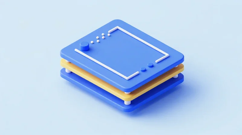
In high-frequency designs, via transitions act as significant discontinuities. To minimize parasitic capacitance and inductance, designers must optimize the return path and minimize the stub length. Implementing optimized via anti-pads and ensuring immediate proximity to ground stitching vias are critical to maintaining signal integrity across layer changes.
The Role of Backdrilling in Signal Integrity
Backdrilling is the controlled-depth drilling process used to remove the unused portion of a via barrel, effectively eliminating the 'stub' that acts as an open-ended transmission line. For data rates exceeding 56Gbps PAM4, even small stubs can cause severe resonance and signal degradation.
| Feature | Impact on Signal | Recommended Practice |
|---|---|---|
| Via Stub Length | High-frequency reflection | Backdrill to <10mil |
| Anti-pad Geometry | Capacitive loading | Simulate for impedance matching |
| Stitching Vias | Return path discontinuity | Maintain <20mil proximity |
Frequently Asked Questions
- Why is backdrilling essential for 112G designs?
At 112G, even a 20-mil stub can create a resonance notch within the operating bandwidth, leading to massive insertion loss. - How does via anti-pad size affect impedance?
Increasing the anti-pad diameter reduces parasitic capacitance, which is necessary to counteract the capacitive loading caused by the via pad in high-layer-count boards. - What are the DFM risks of backdrilling?
Primary risks include drill wander and potential damage to internal signal layers; therefore, strict drill-to-layer clearances must be maintained.
Thermal Management for High-Density Switches
Thermal-Signal Integrity Synergy
In modern data center switches, thermal management is not merely a mechanical concern; it is a primary driver of signal integrity (SI). As ASIC power density exceeds 500W, localized heat can cause dielectric constants (Dk) and dissipation factors (Df) to drift, leading to phase shifts and increased insertion loss. Managing this requires a holistic approach that integrates thermal dissipation directly into the PCB stack-up design.
Material Selection and Heat Distribution
The choice of high-frequency substrate materials must balance dielectric performance with a high Glass Transition Temperature (Tg). PCBs operating at 112G and 224G PAM4 require laminates that remain stable under prolonged thermal cycling to prevent via micro-cracking and impedance instability.
| Thermal Strategy | SI Impact | Implementation |
|---|---|---|
| Thermal Vias | Minimized Hotspots | Array of copper-filled vias under ASIC |
| Heavy Copper Planes | Uniform Heat Spreading | Use of 2oz+ internal layers |
| Low-CTE Laminates | Reduced Mechanical Stress | Ceramic-filled high-frequency resins |
Best Practices for Thermal Design
- How do thermal vias affect SI?
Thermal vias can introduce parasitic capacitance and inductance if placed too close to high-speed signal transitions. Ensure that thermal via patterns maintain a 'keep-out' distance from signal vias to prevent impedance discontinuities. - Why is copper thickness critical for heat?
Increased copper weight improves lateral thermal conductivity, acting as a heat spreader to move thermal energy away from the ASIC core and towards heat sink interfaces. - What role do thermal interface materials (TIM) play?
TIM selection must match the thermal expansion characteristics of the PCB to ensure consistent contact pressure, preventing air pockets that would otherwise lead to localized thermal runaway.
Validation: Simulation vs. Reality
The Simulation-to-Reality Calibration Gap
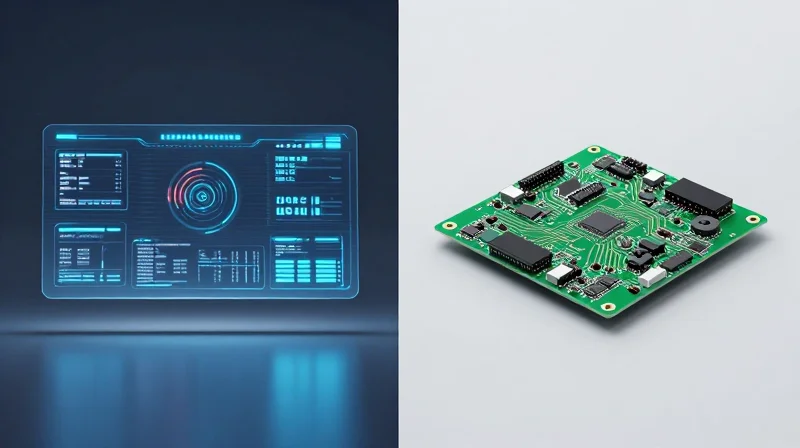
While electromagnetic (EM) solvers provide highly accurate predictions, discrepancies often arise due to manufacturing tolerances and material inconsistencies. To bridge this gap, engineers must correlate simulated S-parameters with measured data from TDR (Time Domain Reflectometry) and VNA (Vector Network Analyzer) testing, ensuring that the 'as-designed' digital twin accounts for real-world dielectric dissipation factors and copper roughness profiles.
Comparison: Simulation Inputs vs. Manufacturing Variables
| Variable | Simulation Assumption | Manufacturing Reality |
|---|---|---|
| Copper Roughness | Idealized smooth surface | Calculated using Huray or Cannonball models |
| Dielectric Constant | Nominal data sheet value | Frequency-dependent shifts and resin flow variation |
| Etch Profile | Perfect rectangular traces | Trapezoidal cross-sections due to undercut |
| Via Geometry | Absolute vertical drilling | Drill wander and plating thickness variance |
Best Practices for Correlation and Validation
- How do you account for copper roughness in models?
Utilize advanced surface roughness models like the Huray model in your solver, as the standard 'ideal conductor' assumption will significantly underestimate insertion loss at 56G and 112G PAM4 speeds. - Why should test coupons be included?
Always integrate dedicated impedance and insertion loss test coupons on the fabrication panel to validate that the manufactured boards match your simulated stack-up requirements before committing to full production. - How can TDR be used for validation?
Perform TDR analysis on the physical prototype to identify specific impedance discontinuities, then map these back to the simulation model to identify where design geometry needs adjustment.
By integrating these iterative validation steps, design teams can create a closed-loop system where simulation data informs manufacturing tolerances, and physical performance data refines future simulation models. This methodology effectively eliminates the 'unknowns' that lead to costly re-spins in high-frequency data center switch hardware.
Achieving success at 800G requires a holistic approach where manufacturing feasibility meets signal integrity excellence. By strictly adhering to these DFM principles and refined SI techniques, you can ensure your switch designs remain competitive and reliable in the face of rising bandwidth requirements. Ready to optimize your high-speed hardware architecture? Contact our engineering team today to review your current PCB stack-up and design constraints.
