
In the fast-paced world of server architecture, scaling your PCB designs to 12-24 layers introduces a host of engineering challenges that can derail production. As signal speeds increase and space becomes a premium, standard design practices often fall short. This guide bridges the gap between complex design requirements and manufacturability, providing you with the DFM insights necessary to ensure high performance and reliability.
The Anatomy of High-Layer Stack-ups
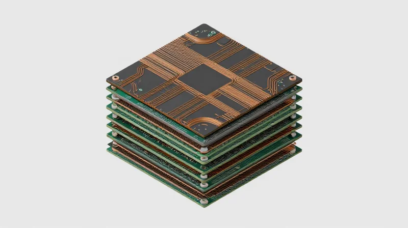
The Imperative of Symmetry
For high-layer count boards, symmetry is the foundational principle for mitigating mechanical deformation. A stack-up must be perfectly balanced regarding copper distribution, dielectric thickness, and material properties across the neutral axis. As layer counts increase beyond 12, the internal stresses induced during the lamination process multiply, making thermal-mechanical stability a critical Design for Manufacturing (DFM) metric.
Layer Distribution and Impedance Control
In 12-24 layer designs, stack-up planning must prioritize signal integrity (SI) by alternating ground planes with signal layers. This prevents coupling and crosstalk while providing a controlled reference environment. The following table highlights common strategy distribution differences for high-performance server boards.
| Board Layer Count | Primary Constraint | Signal/Plane Strategy |
|---|---|---|
| 12 Layers | Board Thickness | 4 Signal / 8 Plane |
| 18 Layers | Signal Integrity | 6 Signal / 12 Plane |
| 24 Layers | Power Delivery | 8 Signal / 16 Plane |
Essential DFM Considerations for Stack-up Design
- How does core and prepreg selection affect warpage?
Utilizing consistent glass-weave styles and matching the Coefficient of Thermal Expansion (CTE) across core layers prevents internal stresses that cause twisting and bowing during reflow. - Why must copper balance be maintained?
Uneven copper distribution creates asymmetric thermal expansion rates during lamination, which directly results in board warpage. Always aim for uniform copper density in both the x and y axes for every layer. - What is the impact of drilling aspect ratios?
For 24-layer boards, the thickness-to-drill-diameter ratio must be considered early. Extremely thick boards increase drill wear and plating difficulties, potentially requiring back-drilling or blind/buried vias to maintain signal performance.
Advanced Impedance Control Strategies

Mitigating Impedance Fluctuations in High-Layer Designs
For server motherboards ranging from 12 to 24 layers, maintaining impedance within a ±5% tolerance requires moving beyond standard design rules. Achieving this necessitates integrated compensation for resin flow, copper thickness variation, and the dielectric constant (Dk) shifts inherent in multi-stage lamination processes.
Dielectric Constant (Dk) and Lamination Strategy
As the layer count increases, the effective Dk of the stack-up often shifts due to the cumulative effects of multiple lamination cycles and variations in resin content. Engineers must utilize material-specific 'etch-back' compensation factors and collaborate with fabricators to characterize the Dk behavior after sequential lamination.
| Variable | Impact on Impedance | DFM Mitigation Strategy |
|---|---|---|
| Copper Thickness | High (Affects cross-section) | Use foil-based copper instead of plated-up for critical signals |
| Resin Flow | Medium (Alters dielectric thickness) | Define restrictive pre-preg patterns and use glass-style control |
| Lamination Cycles | High (Dk degradation) | Characterize material post-lamination; apply compensation factors |
Advanced Impedance Control FAQ
- How does sequential lamination affect impedance?
Each heat cycle changes the resin flow and material thickness; designers must perform post-lamination coupons measurements to adjust trace widths in subsequent build-up layers. - Is trace width compensation sufficient for tight tolerance?
No, trace width compensation alone is insufficient. You must also account for etching factor variations and dielectric glass-weave effects to ensure signal integrity across 24 layers. - What is the role of TDR testing in DFM?
Time Domain Reflectometry (TDR) is essential for verifying impedance profiles against design targets, allowing for real-time calibration of etching processes during high-volume production.
Via-in-Pad and Microvia Best Practices
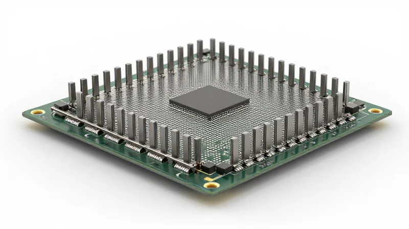
Via-in-Pad and Microvia Best Practices
For 12-24 layer server motherboards, via-in-pad (VIPPO) is not merely a design choice but a requirement for high-density breakout patterns (BGA). However, improper implementation introduces significant risks, including copper voids during assembly, potential outgassing, and exacerbated crosstalk. Engineers must mandate conductive or non-conductive via filling followed by planarized copper capping to ensure a flat soldering surface and to prevent solder wicking into the barrel.
Strategic Microvia Implementation
Microvias (typically laser-drilled, diameter < 150µm) are critical for escaping high-pin-count processors. Adopting an HDI (High-Density Interconnect) strategy with stacked or staggered microvia structures is essential. To ensure reliability in thick high-layer counts, focus on aspect ratio limits (generally 1:1 for reliable copper plating) and prioritize stacked vias only when the laminate thermal expansion coefficients (CTE) are perfectly matched.
| Feature | Recommendation for 12-24 Layers | DFM Impact |
|---|---|---|
| Via Plugging | Epoxy Fill + Copper Cap | Prevents solder theft; ensures flat BGA pads |
| Microvia Ratio | Maximum 1:1 Aspect Ratio | Ensures void-free plating in high-stress thermal cycles |
| Staggered vs Stacked | Prefer Staggered | Reduces cumulative stress on the copper barrel |
Frequently Asked Questions
- Why is copper capping mandatory for via-in-pad?
Without a planarized copper cap, solder will wick down the via barrel during reflow, creating an insufficient joint at the BGA pad and potentially trapping flux residue that causes long-term corrosion. - How do microvias affect impedance in 20+ layer boards?
Microvias create small capacitive discontinuities. Minimize their impact by ensuring the stub length is effectively zero and by maintaining a consistent reference plane transition to avoid impedance mismatch. - What is the primary risk of stacked microvias?
Stacked microvias are prone to barrel cracking due to CTE mismatch during thermal cycling. Use only when required for routing density and specify high-Tg (Glass Transition Temperature) materials to improve reliability.
Addressing Signal Integrity at 56G and Beyond

Mitigating High-Frequency Insertion Loss
At 56G PAM4 and higher, insertion loss is dominated by dielectric dissipation and copper surface roughness. Designers must transition to ultra-low-loss (ULL) materials characterized by a dissipation factor (Df) below 0.002. Minimizing copper roughness—specifically using HVLP (Hyper Very Low Profile) or VLP (Very Low Profile) foils—is mandatory to reduce skin-effect losses that become critical as signal energy propagates through high-layer counts.
Dielectric and Copper Selection Comparison
| Material Category | Df (at 10GHz) | Copper Profile | Primary Application |
|---|---|---|---|
| Standard FR-4 | 0.015 - 0.020 | Standard | Low-speed control |
| Mid-Loss Laminate | 0.008 - 0.010 | Low Profile | 10G Base-T |
| Ultra-Low Loss (ULL) | < 0.002 | HVLP | 56G/112G PAM4 |
Design Guidelines for Reflection Control
Reflections caused by impedance discontinuities are the primary performance killers in 12-24 layer server boards. At 56G frequencies, even minor geometry changes at via transitions create significant return loss. Maintaining a strict ground reference planarity and utilizing back-drilling techniques for all high-speed vias is no longer optional; it is a fundamental requirement.
- How does trace geometry impact 56G signals?
Traces must maintain strict width uniformity to avoid characteristic impedance variations; even 0.5-mil deviations lead to localized impedance spikes that trigger reflections at high Nyquist frequencies. - Why is back-drilling critical for high-layer stacks?
Stubs create resonant frequencies that act as notch filters. Back-drilling removes the parasitic capacitive loading of unused via barrels, extending usable bandwidth significantly. - What role does weave effect play?
Fiber-weave skew causes phase mismatch in differential pairs, resulting in intra-pair skew. Designers must use 'spread glass' weave styles or rotate the PCB design by 10 degrees to average out the glass/resin ratio.
Managing Thermal Dissipation in Dense Architectures
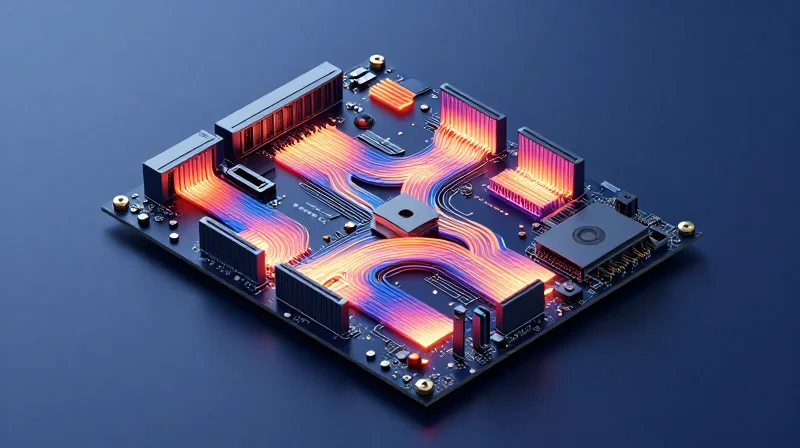
Managing Thermal Dissipation in Dense Architectures
In server motherboards exceeding 12 layers, the primary thermal challenge is the migration of heat from high-TDP processors and VRM modules to the external environment. Designers must treat the PCB not merely as an interconnect medium, but as a primary heat sink, utilizing plane layers as thermal spreaders to mitigate localized hotspots that threaten long-term component reliability.
Copper Plane Optimization for Heat Spreading
To maximize dissipation efficiency, internal copper planes should be designed with low thermal resistance paths. Increasing copper weight on inner power layers to 2oz or higher is recommended for critical heat-generating areas, provided it does not compromise impedance control for high-speed signal layers.
| Strategy | Primary Goal | DFM Consideration |
|---|---|---|
| Thermal Vias | Vertical heat transfer | Maintain grid pitch to avoid plane fracturing |
| Copper Pours | Lateral heat spreading | Ensure balancing to prevent board warpage |
| Component Staggering | Uniform heat distribution | Maintain clearance for assembly rework |
Thermal Via Array Engineering
Thermal via arrays must be placed directly beneath the thermal pads of high-power ICs. To optimize performance, utilize a standard 0.2mm - 0.3mm drill size with copper filling. This reduces thermal resistance significantly while ensuring consistent plating thickness for structural integrity during thermal cycling.
- What is the optimal pitch for thermal via arrays?
A pitch of 0.8mm to 1.2mm is standard to balance thermal conductivity with the need to maintain sufficient plane integrity for power delivery. - How does layer count impact heat dissipation?
Higher layer counts offer more potential planes for heat spreading; however, increased dielectric thickness can act as an insulator, making the strategic placement of thermal vias more critical. - Can solder mask thickness affect cooling?
Yes, excessive solder mask thickness acts as an insulator; using mask-defined pads or limiting mask coverage on thermal relief areas can improve heat transfer to heat sinks.
DFM Rules for High-Yield Assembly
Ensuring Precision in High-Layer Count Assembly
In 12-24 layer server motherboards, assembly yields are heavily dependent on managing the interaction between fabrication tolerances and surface mount technology (SMT) processes. Achieving high yields requires a collaborative approach with your PCB fabricator to define acceptable drill-to-copper clearances and annular ring integrity before designs move to production.
Critical DFM Parameters for Fabrication and Assembly
| Feature | Design Constraint (12-24 Layer) | Impact on Assembly Yield |
|---|---|---|
| Annular Ring | Minimum 50-75µm | Prevents via breakout during thermal cycling |
| Drill-to-Copper | Minimum 200-250µm | Avoids shorts between signal layers and power planes |
| Solder Mask Web | Minimum 75µm | Prevents solder bridging on dense BGA footprints |
Collaboration Strategies with Fabricators
- How do I ensure drill-to-copper clearance compliance?
Perform pre-layout stack-up reviews with your fabricator to account for layer misregistration limits. Always budget for the worst-case registration tolerance provided by the manufacturer. - What is the best way to handle annular ring requirements?
Utilize non-functional pad removal (NFPR) for inner layers to reduce capacitive coupling, but ensure the fabricator's drill tolerance is explicitly factored into the remaining ring calculation. - How can I improve SMT yield on dense BGA arrays?
Define solder mask defined (SMD) vs. non-solder mask defined (NSMD) pads based on the specific thermal expansion coefficient of the board material and component package to ensure robust solder joints.
To guarantee success, incorporate design-for-test (DFT) access points and specify gold plating integrity for connectors early in the cycle. By aligning your design constraints with the fabricator's manufacturing capabilities—specifically focusing on drill alignment and plating thickness—you significantly mitigate the risk of intermittent failures during the server motherboard assembly process.
Material Selection: Beyond Standard FR-4
Beyond FR-4: The Shift to Ultra-Low-Loss Laminates
Standard FR-4, while cost-effective for low-speed designs, fails to meet the stringent dielectric constant (Dk) and dissipation factor (Df) requirements of 12-24 layer server backplanes. At 56G PAM4 and beyond, the dielectric loss tangent becomes the primary bottleneck. Engineers must migrate toward high-performance thermoset resins and PTFE-based substrates, such as Megtron 6, Megtron 7, or Tachyon 100G, which offer consistent impedance control and superior thermal reliability across massive multi-layer stacks.
Comparison of High-Speed Substrate Materials
| Material Class | Df (at 10GHz) | Application Focus | Thermal Reliability |
|---|---|---|---|
| Standard FR-4 | 0.020 | Legacy/Low Speed | Moderate |
| Mid-Loss Laminate | 0.010 - 0.012 | PCIe Gen 3/4 | High |
| Ultra-Low Loss | 0.002 - 0.004 | 56G/112G SerDes | Very High |
Key Design Considerations for Advanced Materials
- How does glass weave affect high-speed signals?
The 'fiber weave effect' causes skew between differential pairs. Engineers must specify 'spread glass' (e.g., 1067 or 1078 styles) to ensure uniform dielectric properties along the trace path. - Why is copper foil roughness a critical parameter?
At high frequencies, the skin effect concentrates current at the copper surface. Using Very Low Profile (VLP) or Hyper-Low Profile (HVLP) copper reduces insertion loss caused by surface irregularities. - What are the DFM implications for material thickness?
Advanced materials often have different drill-to-copper expansion coefficients; always verify the Z-axis CTE of your chosen material to prevent barrel cracking in high-aspect-ratio vias.
When transitioning to these materials, always coordinate with your fabricator regarding the 'stack-up availability' and lead times, as specialized ultra-low-loss materials often require unique pre-preg bonding cycles that differ significantly from standard manufacturing workflows.
Post-Layout Verification and Simulation
The Necessity of Advanced Post-Layout Verification
For 12-24 layer server motherboards, pre-manufacturing validation must transcend basic connectivity checks. It involves rigorous electromagnetic (EM) analysis and Design Rule Check (DRC) cycles to identify potential failures in signal integrity, power distribution network (PDN) stability, and mechanical DFM tolerances that standard EDA checks might overlook.
Key Simulation and Verification Domains
| Verification Type | Primary Objective | Critical Metric |
|---|---|---|
| EM Simulation | Identify crosstalk and EMI hotspots | Decibel (dB) margin |
| PDN Analysis | Verify IR drop and impedance | Millivolt (mV) ripple |
| DRC/DFM Audit | Validate etch and drill clearances | Aspect Ratio compliance |
Frequently Asked Questions
- Why is 3D EM simulation required for high-layer count designs?
As layer counts increase, vertical transitions (vias) become significant antennas. 3D EM simulation allows engineers to optimize via stubs and back-drilling depths, which are essential for signal integrity in designs exceeding 10Gbps. - How does automated DRC differ from manual DFM inspection?
Automated DRC ensures adherence to basic design rules, but specialized DFM auditing flags complex manufacturing risks, such as acid traps, non-conductive via tenting issues, and localized copper density imbalances that affect plating uniformity. - What is the role of IR drop simulation in power integrity?
IR drop simulation predicts voltage degradation across the power planes of a 24-layer board, ensuring that critical high-current components receive the required voltage under transient load conditions to prevent system resets.
By integrating these verification steps into the design flow, engineering teams effectively shift the failure detection earlier, drastically reducing the probability of multiple board respins and accelerating the time-to-market for high-density server platforms.
Designing 12-24 layer server motherboards is a complex balancing act between electrical performance and physical manufacturability. By adhering to these DFM best practices, you can minimize production cycles, reduce costly re-spins, and deliver superior hardware performance. Ready to optimize your next high-speed design? Contact our engineering team today to review your stack-up and design requirements.
