
As data center bandwidth demands skyrocket to 800G and beyond, the margin for error in signal integrity vanishes. Designers are no longer just fighting noise; they are fighting physics. To maintain signal fidelity at these blistering speeds, a fundamental shift in Design for Manufacturing (DFM) is required. This guide explores the critical bridge between theoretical signal integrity and real-world manufacturing excellence.
The Physics of 800G: Why Traditional DFM Falls Short

The 800G Paradigm Shift
At 800G speeds, copper traces and dielectric materials no longer behave as static components but as complex transmission lines where signal degradation is an inherent factor of geometry. Traditional DFM guidelines, focused primarily on mechanical clearance and basic manufacturing tolerances, fail to account for the non-linear relationship between signal frequency and material response.
Critical Physical Impediments
| Physical Phenomenon | 800G Impact | DFM Limitation |
|---|---|---|
| Skin Effect | High current density at conductor surface | Standard plating thickness ignores surface roughness |
| Dielectric Absorption | Increased signal loss and phase jitter | Standard FR-4 is lossy at these frequencies |
| Insertion Loss | Severe amplitude reduction | Insufficient trace impedance control |
As we push toward higher PAM4 signaling, the skin effect necessitates ultra-smooth copper foils to mitigate high-frequency loss. Traditional DFM often allows for standard-grade copper that exacerbates parasitic inductance, causing unacceptable signal dispersion at the 112Gbps-per-lane threshold required for 800G systems.
Frequently Asked Questions
- Why does dielectric loss matter more at 800G?
Higher frequencies translate into shorter wavelengths where the material's dissipation factor directly dictates the signal's ability to maintain its integrity over even short trace lengths. - Is standard PCB fabrication still viable?
No, standard fabrication often lacks the precision in laser drilling and copper plating uniformity needed to suppress the electromagnetic interference prevalent at 800G bandwidths. - How does DFM need to evolve?
DFM must shift from mechanical design rules to electromagnetic-centric rules, incorporating co-simulation between layout and field solvers to predict high-frequency losses before manufacturing.
Strategic Material Selection for High-Frequency Substrates
The Imperative for Low-Loss Dielectrics
As signaling rates transition from 112G to 224G, the traditional PCB material framework encounters significant performance ceilings. Signal attenuation is primarily driven by dielectric loss (Df) and copper surface roughness. At these frequencies, even minor fluctuations in the dielectric constant (Dk) can lead to significant impedance discontinuities and unacceptable insertion loss. Engineers must prioritize substrates with ultra-low Dk (typically below 3.0) and Df (below 0.002) to maintain a robust power-to-signal budget.
| Parameter | Standard FR-4 | High-Speed Laminate (800G/224G) | Impact on Performance |
|---|---|---|---|
| Dk (at 10GHz) | 4.4 - 4.8 | 2.9 - 3.2 | Reduces signal phase delay |
| Df (at 10GHz) | 0.020 | < 0.002 | Minimizes dielectric absorption |
| Thermal Stability | Moderate | Excellent (High Tg) | Reduces micro-via stress |
Mitigating Copper Loss and Skin Effect
Beyond the dielectric medium, the interface between copper and substrate is a primary source of high-frequency attenuation. At 224G, the 'skin effect' forces current to flow through the surface irregularities of the copper foil. Utilizing Very Low Profile (VLP) or Hyper-Low Profile (HVLP) copper is non-negotiable for 800G designs to minimize surface roughness-induced impedance scattering.
Strategic Material Selection FAQ
- How does Dk consistency affect 800G interconnects?
Variation in Dk across the PCB surface causes skew in differential pairs, leading to increased eye-diagram closure and higher Bit Error Rates (BER) at high PAM4 signaling speeds. - Why is glass-weave effect a major DFM concern?
The heterogeneous nature of glass fiber bundles can lead to localized Dk differences. Using spread-glass fabrics or non-woven substrates mitigates these effects, ensuring uniform signal propagation timing. - Is moisture absorption a critical factor?
Yes, water has a high Dk. Materials with low moisture absorption indices prevent Dk drift, ensuring the transceiver maintains reliable operation across varying environmental conditions.
Precision Impedance Matching at the Micro-Scale
Precision Impedance Matching at the Micro-Scale
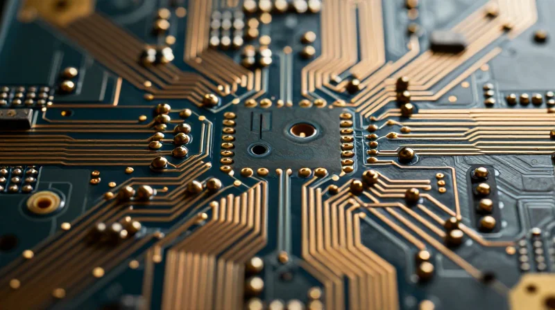
At 800G speeds, where SerDes rates reach 112G and 224G PAM4, the margin for impedance mismatch is virtually non-existent. Standard DFM rules are insufficient because they ignore the secondary effects of copper surface topography and microscopic manufacturing deviations. To maintain a strict 85Ω or 100Ω target, designers must transition from simple geometric modeling to a holistic approach that integrates electromagnetic simulation with real-time manufacturing process feedback.
Mitigating Copper Foil Roughness Effects
The skin effect becomes increasingly problematic as signal frequencies rise, forcing current flow into the microscopic peaks and valleys of the copper-dielectric interface. Standard copper treatments increase surface roughness (Rz), which adds significant resistive losses and effectively changes the inductive behavior of the trace. Utilizing low-profile (LP) or very-low-profile (VLP) copper foil is essential to minimize the 'effective' increase in trace length and maintain impedance stability.
| Feature | 800G Impact | DFM Mitigation Strategy |
|---|---|---|
| Copper Roughness | Increased skin effect loss | Specify VLP or HVLP copper |
| Trace Width Variation | Impedance discontinuity | Tighten tolerance to ±5% or less |
| Etch Factor | Trapezoidal cross-section | Adjust photolithography for vertical sidewalls |
Manufacturing Tolerances and FAQ
- How do manufacturing tolerances affect 800G impedance?
Small variations in trace width, substrate thickness, and copper thickness aggregate at high frequencies, leading to return loss spikes that degrade the Signal-to-Noise Ratio (SNR). - What is the role of etch compensation in high-frequency designs?
Etch compensation must be calculated to account for side-etching, ensuring the final copper geometry matches the modeled width required to maintain exact characteristic impedance. - Why is dielectric uniformity critical?
Localized variations in resin content or glass-weave style cause impedance 'bouncing' along the trace, leading to inter-symbol interference at higher data rates.
Minimizing Insertion Loss via Advanced Via Design
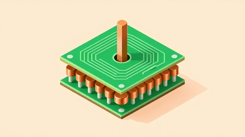
At 800G transmission rates, the via represents one of the most critical points of impedance mismatch in the signal path. The parasitic capacitance of the via barrel and the inductance of the remaining 'stub' create resonance effects that severely degrade return loss and contribute to excessive insertion loss. Mitigating these effects requires moving beyond standard PCB design practices toward controlled-depth drilling and geometric optimization.
Mitigation Techniques for Via-Induced Losses
- Back-drilling
Controlled-depth drilling of the unused portion of a via barrel eliminates the resonant stub, preventing signal reflections that typically appear as notches in the frequency response above 20 GHz. - Via Stitching and Grounding
Strategically placing ground vias in proximity to signal vias provides a continuous return path, lowering the loop inductance and preventing electromagnetic field discontinuities. - Staggered Via Structures
Utilizing staggered or micro-via-in-pad structures allows for tighter routing density while maintaining a controlled impedance profile across layer transitions.
| Via Technique | Primary Benefit | Design Constraint |
|---|---|---|
| Back-drilling | Eliminates stub resonance | Drill depth tolerance (±2-3 mil) |
| Stitched Ground Vias | Reduces return path impedance | Minimum clearance (keep-out) rules |
| Micro-via Structures | Minimizes parasitic capacitance | Sequential lamination complexity |
Advanced Via Optimization Workflow
Designers must perform 3D electromagnetic (EM) modeling to optimize the pad diameter and anti-pad (clearance) geometry of the via transition. By increasing the anti-pad size, the designer can reduce the parasitic capacitance against the reference planes, effectively 'tuning' the via to maintain a 50-ohm characteristic impedance profile at 112G and 224G PAM4 signaling thresholds.
via_design_parameters = {
  'stub_length': '0 mil',
  'anti_pad_shape': 'circular',
  'ref_plane_clearance': '12 mil',
  'signal_to_ground_ratio': '1:1'
}
Optimizing Trace Routing and Geometry
Optimizing Trace Routing and Geometry
At 800G data rates utilizing 112G and 224G PAM4 signaling, trace routing must shift from traditional design methodologies to precision electromagnetic management. Effective routing requires tight control over differential pair symmetry, coupled with sophisticated geometric compensation to counteract the effects of weave-induced skew and dielectric anisotropy.
Mitigating Skew and Crosstalk
Signal integrity in 800G systems is highly sensitive to intra-pair skew, where the arrival time difference between differential signals degrades the eye diagram. Implementing 'zig-zag' routing patterns and utilizing rounded trace corners can significantly reduce reflections. Furthermore, increasing the spacing between adjacent differential pairs is essential to suppress Far-End Crosstalk (FEXT) in dense high-speed routing regions.
| Routing Parameter | Best Practice for 800G | Impact |
|---|---|---|
| Trace Cornering | Use curved/rounded traces | Reduces impedance discontinuities |
| Intra-pair Skew | Phase compensation near source | Synchronizes signal timing |
| Adjacent Pair Spacing | Minimum 3x dielectric height | Minimizes crosstalk energy |
| Reference Planes | Continuous solid ground planes | Controls return path inductance |
Frequently Asked Questions on Routing Best Practices
- How does PCB weave affect high-speed routing?
Fiber-weave effect causes periodic variations in effective dielectric constant, leading to phase shifts. Routing traces at a slight angle to the weave or using spread-glass laminates mitigates this risk. - Why should we avoid right-angle bends in 800G traces?
Right-angle bends introduce parasitic capacitance at the corner, creating impedance mismatches that manifest as high-frequency reflections. Rounded geometries ensure a smoother transition for the electromagnetic wave. - Is layer transition necessary for routing density?
While necessary for density, every via adds discontinuity. Minimize layer changes; if required, use optimal back-drilling and ensure symmetrical stitching vias to maintain return path continuity.
Manufacturing Process Controls: From CAD to FAB

Establishing Tight Process Windows for 800G Reliability
Transitioning from CAD to fabrication at 800G requires narrowing the manufacturing process windows to accommodate high-frequency signal integrity requirements. Engineers must collaborate with fabricators to define precise etching profiles and dielectric thickness tolerances that mitigate performance drift caused by production variability.
Controlling Etch Uniformity and Dielectric Thickness
At 800G, even minor deviations in trace width or dielectric height cause significant impedance discontinuities. To maintain the requisite performance, manufacturers must employ advanced control techniques such as pulse plating for uniform copper deposition and laser-direct imaging (LDI) for superior etching precision.
| Control Metric | Typical Tolerance (800G) | Manufacturing Technique |
|---|---|---|
| Trace Width | +/- 5% | LDI & Modified Semi-Additive |
| Dielectric Thickness | +/- 3% | Vacuum Lamination |
| Copper Roughness | Ra < 0.2um | Low-Profile VLP/HVLP Foils |
Frequently Asked Questions: Manufacturing DFM
- How does copper foil roughness impact 800G signals?
Higher surface roughness increases the skin effect at high frequencies, leading to excessive insertion loss; VLP (Very Low Profile) foils are essential to minimize this impact. - Why is vacuum lamination critical for dielectric thickness?
Vacuum lamination minimizes resin flow variations and air entrapment, ensuring the dielectric constant (Dk) remains uniform across the high-speed signal path. - What is the primary benefit of LDI over traditional photolithography?
LDI eliminates mask-induced errors, allowing for finer line definition and tighter registration control, which are vital for complex 800G multi-layer stack-ups.
Testing and Validation for High-Speed Reliability

Core Characterization Methodologies
At 800G speeds, the margin for error is minimal, requiring a transition from functional pass/fail testing to full parametric characterization. Validation must focus on isolating impedance discontinuities, managing insertion loss, and ensuring jitter performance remains within strict SerDes thresholds.
| Methodology | Target Parameter | Significance for 800G |
|---|---|---|
| TDR Analysis | Impedance Profile | Identifies discontinuities from vias and connectors. |
| VNA Analysis | S-Parameters (Sdd21, Sdd11) | Maps frequency-domain loss and return loss. |
| Eye Diagram | Jitter/Eye Height/Width | Confirms signal integrity and BER performance. |
Frequency and Time-Domain Validation Strategies
Time Domain Reflectometry (TDR) is critical for diagnosing the physical layout, specifically detecting impedance fluctuations caused by inadequate via stubs or imperfect trace geometries. Once the layout is verified, Vector Network Analyzer (VNA) sweeps provide essential data on channel insertion loss (IL) and return loss (RL). For 800G systems, the validation must extend beyond the fundamental frequency to account for harmonics affecting higher-order PAM4 signaling.
Production Yield Verification FAQ
- How does PAM4 signaling change testing requirements?
PAM4 uses four levels, resulting in a signal-to-noise ratio (SNR) that is 9.5 dB worse than NRZ; therefore, validation must focus on precise linearity and noise-floor suppression. - Why is S-parameter de-embedding necessary?
De-embedding removes the influence of test fixtures and cables from the measurement, ensuring the results reflect only the transceiver PCB performance. - What is the primary indicator of failure in 800G testing?
Excessive jitter and eye closure due to inter-symbol interference (ISI) caused by improper termination or resonance typically indicate assembly or fabrication process drifts.
Future-Proofing Designs for the 1.6T Era
The Architectural Shift toward 1.6T
The evolution from 800G to 1.6T is not merely a scaling exercise but a fundamental transition in how optical engines interface with host ASICs. At these data rates, traditional pluggable form factors face insurmountable signal integrity and power density bottlenecks. Designers must shift toward co-packaged optics (CPO) and silicon photonics to reduce electrical path lengths, thereby mitigating insertion loss that would otherwise cripple 200Gbps-per-lane signaling.
Design Constraints and Mitigations
| Challenge | 800G Best Practice | 1.6T Future Adaptation |
|---|---|---|
| Signal Path | Minimized PCB Traces | Silicon Photonics / CPO |
| Thermal Density | Advanced TIM and Heat Sinks | Liquid Cooling / Microfluidics |
| Modulation | PAM4 | Higher-order Modulation or Parallelism |
Future-Proofing Through Thermal Management
Thermal management remains the primary constraint for 1.6T transceivers. As power consumption increases, conventional forced-air cooling reaches a point of diminishing returns. Engineers should prepare for next-generation packaging that utilizes integrated micro-channel cooling or direct-to-chip liquid cooling systems. Building modularity into the PCB stackup now allows for the later integration of these high-performance cooling architectures without requiring a full redesign of the high-speed signaling layers.
FAQs on 1.6T Manufacturing Readiness
- How will 1.6T change PCB material requirements?
Designers will need to adopt even lower-loss ultra-thin laminates and potentially move to glass-based substrates to maintain signal integrity at higher frequency harmonics. - Is pluggable optics still viable at 1.6T?
While pluggables will persist for specific reach applications, the industry is trending toward CPO to solve the 'reach vs. power' trade-off inherent in high-density copper interconnects. - What is the biggest DFM shift for the next era?
The integration of optical and electrical testing during the manufacturing process—rather than separate post-production testing—will be critical to maintaining yields.
Successfully deploying 800G optical transceivers requires a holistic approach that integrates advanced materials, rigorous impedance control, and optimized manufacturing processes. By implementing these DFM best practices, your team can ensure superior signal integrity and high production yields. Ready to elevate your hardware performance? Contact our engineering team today to review your current design files and integrate next-generation manufacturing strategies.
