
In the fast-paced world of autonomous robotics, the printed circuit board is the heart of the system. Designing for high-density navigation sensors like LiDAR and VSLAM requires a delicate balance between miniaturization and thermal reliability. This guide provides an expert roadmap to optimizing your design for manufacturing (DFM) processes, ensuring your robot vacuums move from prototype to mass production with minimal defects.
Understanding High-Density Interconnect (HDI) Requirements
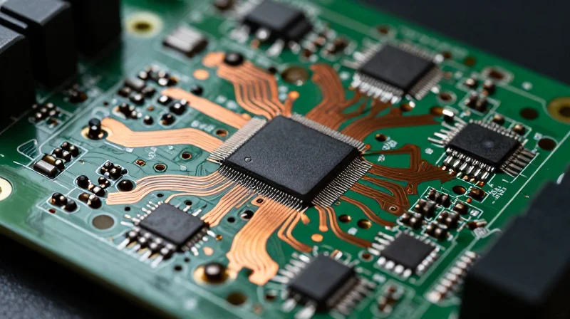
As robot vacuums evolve from simple sweepers to sophisticated autonomous units featuring LiDAR, advanced SLAM algorithms, and multi-sensor fusion, the demand for compact and high-performance PCBAs has skyrocketed. HDI technology addresses these space constraints by utilizing finer lines, tighter spacing, and micro-via structures that allow for a much higher connection density per square inch compared to traditional multilayer boards.
Core HDI Design Parameters
For robotic vacuum electronics, engineers must balance signal integrity with manufacturing yield. The following table illustrates the typical design thresholds for moving from standard PCB manufacturing to HDI processing.
| Feature | Standard PCB (mil) | HDI Design (mil) |
|---|---|---|
| Trace Width | 5.0 - 8.0 | 2.0 - 3.5 |
| Trace Spacing | 5.0 - 8.0 | 2.0 - 3.5 |
| Via Diameter | > 8.0 | < 6.0 |
Micro-Via Technology and Assembly Strategy
Micro-vias are critical for routing signals between layers in high-density zones. In robot vacuum motherboards, 'via-in-pad' technology is often employed to save board surface area under fine-pitch BGAs. However, this requires laser-drilled vias and reliable copper plating processes to prevent assembly defects such as solder voids or outgassing during reflow.
HDI Design FAQ
- Why is HDI necessary for sensor-heavy vacuum robots?
Modern vacuums require dense sensor arrays and powerful microcontrollers; HDI allows designers to condense this high pin-count circuitry into a form factor that fits inside a compact robot chassis. - What are the common manufacturing challenges with HDI?
The primary risks include registration alignment between layers and thermal cycling stress on micro-vias, both of which require strict adherence to DFM standards regarding drill-to-copper clearances. - How does HDI influence automated assembly?
HDI designs typically use smaller components (0201 or 01005 passives) and fine-pitch ICs, necessitating higher precision placement equipment and refined solder paste stenciling processes.
Integrating LiDAR and VSLAM Systems

Optimizing Signal Integrity for High-Frequency Sensors
Integrating LiDAR and VSLAM modules introduces complex signal integrity challenges due to the high-frequency nature of CMOS image sensors and motor control PWM interference. To maintain data packet integrity, differential pairs for camera interfaces such as MIPI CSI-2 must be tightly controlled with precise impedance matching of 100 ohms. Any discontinuity in these paths—often caused by poorly placed vias or inconsistent reference planes—will result in packet loss and system-wide synchronization errors.
Noise Mitigation and Shielding Strategies
Electromagnetic interference (EMI) is the primary obstacle when placing high-speed imaging sensors near high-current motor drivers. Implement the following physical design rules to ensure robust sensor performance:
- Localized Ground Islands
Utilize dedicated analog ground planes for sensor sensitive components, isolated from digital grounds via a single-point star connection to prevent return current crosstalk. - Shielding Can Integration
Design footprints for surface-mount shielding cans over the VSLAM processor and MIPI routing to mitigate radiated emissions from the main system clock. - Via Stitching
Implement dense via stitching around the perimeter of high-speed sensor signal layers to create a Faraday cage effect, effectively suppressing lateral electromagnetic noise.
Design Guidelines for Sensor Integration
| Requirement | Recommended Practice | DFM Impact |
|---|---|---|
| Impedance Control | 100Ω Differential (MIPI) | Requires specific stack-up verification |
| Trace Separation | 3x Dielectric Height | Increases total board footprint |
| Via Placement | Avoid via stubs | Mandates back-drilling or blind vias |
| Power Filtering | Ferrite beads at pins | Increases component count |
Frequently Asked Questions
- How can I reduce interference from the laser diode in the LiDAR unit?
Place the laser driver circuitry on the underside of the PCB directly beneath the emitter and isolate the supply lines with a ferrite bead and bulk capacitance to decouple high-frequency ripples. - Do I need blind vias for VSLAM module routing?
While not strictly mandatory, blind vias significantly reduce parasitic capacitance in high-speed traces, which is critical for maintaining high frame rates in dense VSLAM systems.
Optimizing DFM Rules for Complex Assemblies
Refining Solder Mask and Pad Geometry
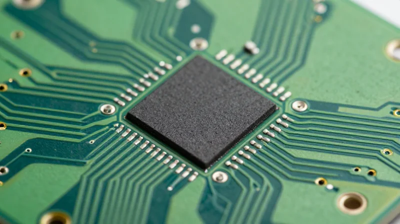
For miniaturized components such as 0201 passives and high-pin-count BGA chips used in vacuum navigation modules, solder mask expansion and pad design are the primary drivers of assembly yield. Incorrect mask-to-pad ratios frequently lead to solder bridging or tombstoning during reflow.
| Feature | Standard Constraint | High-Density Optimization |
|---|---|---|
| Solder Mask Expansion | 0.10mm | 0.05mm - 0.075mm |
| Mask Web (Bridge) | 0.15mm | 0.10mm |
| Pad-to-Pad Spacing | 0.20mm | 0.15mm |
Component Clearances and Automated Assembly Constraints
Automated pick-and-place machines require specific keep-out zones and orientation clearances to avoid mechanical interference during high-speed nozzle movement. In robot vacuum PCBAs, the integration of bulky battery connectors alongside sensitive sensors mandates a tiered clearance strategy.
- How do I mitigate shadowing effects in reflow?
Avoid placing tall, large-mass components (such as electrolytic capacitors) immediately upstream of smaller components in the direction of the reflow oven airflow to prevent uneven solder melting. - What is the critical clearance for automated inspection?
Ensure a minimum 0.5mm clearance around all high-density ICs to allow for AOI (Automated Optical Inspection) camera angles, preventing 'blind spots' that could mask solder joint defects. - Why is copper balancing critical for assembly?
Asymmetric copper distribution causes PCB warping during thermal cycles. Use non-functional copper pours to ensure uniform thermal expansion, preventing misalignment during automated placement.
Best Practices for Pad-in-Via Technology
if (via_in_pad) {
  apply_conductive_fill();
  perform_planarization();
  check_solder_mask_coverage(min_clearance = 0.025);
}
When using via-in-pad for high-density BGA routing, ensure all vias are filled with conductive epoxy and capped with copper plating. This prevents solder wicking, which creates 'solder starvation' at the joint, a common failure mode in robot vacuum power management boards.
Thermal Management in Compact Enclosures
Thermal Management in Compact Enclosures
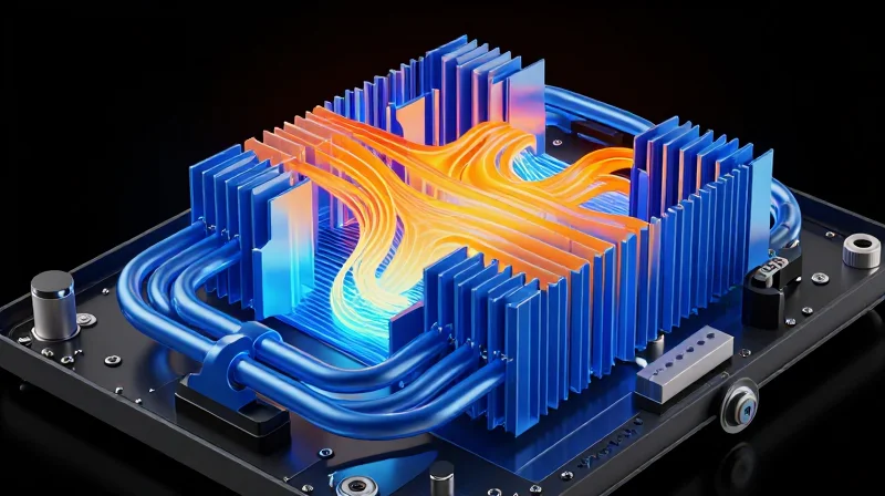
In the confined chassis of a robot vacuum, heat density from high-performance application processors and motor controllers poses a critical risk to component longevity. Designers must move beyond passive cooling by treating the PCBA as a functional heat spreader, utilizing thermal vias, copper pours, and strategic component placement to shunt heat toward the chassis surface or internal heatsinks.
Heat Dissipation Strategies for High-Load Components
| Component Type | Heat Characteristic | Recommended Strategy |
|---|---|---|
| Application Processor (CPU) | High continuous thermal output | Thermal vias to internal ground plane + TIM |
| Motor Controller (MOSFETs) | High peak switching current | Thick copper traces + heatsink coupling |
| Wireless/RF Modules | Low-level continuous heat | Airflow channels + shielding heat sinking |
To ensure maximum efficiency, place high-thermal-load components near the perimeter of the PCBA where they can interface directly with the robot's plastic enclosure via thermally conductive pads (TIM). Avoid grouping high-heat components; spatial distribution is essential to prevent hot-spot formation that could lead to PCB warping during reflow or operational failure.
Thermal Design FAQ
- Why is thermal via density critical for vacuum PCBA design?
Thermal vias provide a vertical path for heat to transfer from component pads into internal copper ground planes, which act as a massive heat sink across the entire board area. - How does PCB thickness influence thermal performance?
While standard 1.6mm boards are common, using 2oz copper weights instead of 1oz significantly increases the thermal conductivity of the board, allowing for better heat spreading without needing bulky external cooling solutions. - Should I use active or passive cooling?
Passive cooling is preferred for reliability in vacuums, but if internal temps exceed 85°C, consider localized airflow ducts or integrated aluminum heat spreaders that leverage the air intake stream from the vacuum motor.
Best Practices for PCBA Component Placement
Streamlining Automated Pick-and-Place Efficiency
To achieve maximum throughput in robot vacuum PCBA assembly, the layout must minimize nozzle travel distance and rotational adjustments. Prioritize a uniform orientation for all passive components to streamline vision alignment processes. Components should be placed in a grid-like fashion to allow the pick-and-place gantry to operate at peak velocity without encountering irregular clearance obstructions.
Strategic Component Zoning
| Zone Type | Primary Consideration | Placement Rule |
|---|---|---|
| High-Frequency/Sensors | EMI Shielding | Keep away from motor driver noise |
| Power/Motor Control | Thermal Dissipation | Heavy copper planes, no sensitive traces |
| Control Logic (CPU) | Signal Integrity | Center of board, minimal via transitions |
Reflow Integrity and Solderability Best Practices
Reflow performance in complex vacuum cleaner PCBA designs is heavily dictated by thermal mass uniformity. Avoid placing large components adjacent to minute passives, as this induces tombstoning due to uneven heat absorption. Always maintain sufficient clearance for rework accessibility and prevent solder bridging during mass reflow.
- Why should high-profile components be grouped?
Grouping high-profile parts together prevents shadowing effects, where taller components block convection air currents, leading to uneven solder joint heating. - How does component density affect automated inspection (AOI)?
High density creates occlusions that prevent AOI cameras from accurately capturing solder joints; maintain a minimum 0.5mm clearance around critical IC pins for optimal inspection coverage. - Is there a preferred sequence for placement?
Place components from smallest to largest to avoid mechanical interference during the mounting process and to protect delicate components from robotic head collisions.
Minimizing Defects through Automated Optical Inspection (AOI)
The Strategic Role of AOI in Robot Vacuum Manufacturing
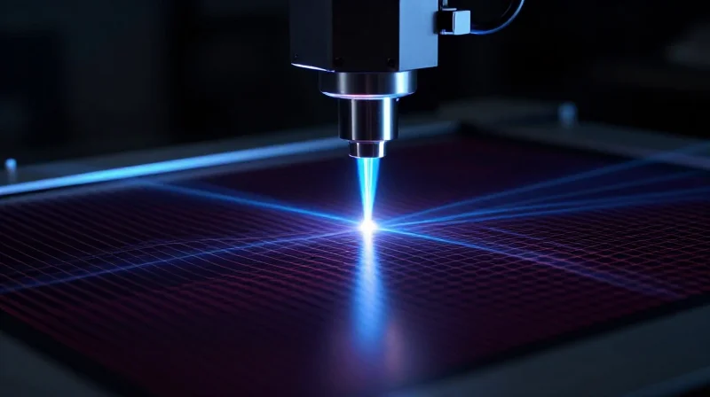
In the context of densely populated robot vacuum mainboards, AOI acts as the primary gatekeeper against common manufacturing defects. By integrating AOI programming directly into the DFM (Design for Manufacturing) phase, engineers can ensure that component footprints are not only optimized for pick-and-place precision but are also fully 'visible' to inspection algorithms. Effective AOI utilization minimizes the escape rate of critical defects such as tombstoning, polarity reversals, and insufficient solder fillets that are common in high-speed, compact electronics.
Design Guidelines for AOI Compatibility
| Design Constraint | AOI Impact | Best Practice |
|---|---|---|
| Component Clearance | Shadowing/Obscuration | Ensure 0.5mm gap between tall capacitors and SMDs. |
| Pad Geometry | Fillet Visibility | Extend pads slightly beyond component body for better inspection. |
| Fiducial Design | Alignment Accuracy | Place 1mm diameter global fiducials at board corners. |
Advanced Inspection: AOI vs. X-Ray
While AOI is highly effective for top-side surface components, complex robot vacuum assemblies—particularly those using BGA (Ball Grid Array) packages for motor controllers—require complementary X-ray inspection to detect hidden soldering issues.
- Why is AOI insufficient for BGA components?
AOI relies on light reflection from solder joints; since BGA solder balls are located underneath the component, they are physically obscured from optical sensors, necessitating X-ray for void analysis. - How does early DFM improve AOI yield?
Standardizing pad geometries and ensuring consistent silkscreen markings reduces 'false calls' in AOI systems, significantly lowering the time required for manual re-inspection. - What is the primary risk of neglecting AOI during design?
Poorly planned AOI access often leads to 'blind spots' where manufacturing defects like solder bridges or dry joints go undetected until the final product fails in the field.
Streamlining Production Throughput and Yield
To achieve high-volume production efficiency for robot vacuum electronics, the bridge between design files and assembly equipment must be seamless. Streamlining throughput requires a proactive approach where design-for-manufacturing (DFM) rules are explicitly mapped to the mechanical and software constraints of the pick-and-place and reflow systems. By establishing a digital thread between the PCB designer and the contract manufacturer, engineers can eliminate the 'design-to-machine' translation lag that frequently causes line stoppages.
Synchronizing Data for Automated Assembly
The primary cause of low assembly yield is the mismatch between CAD outputs and machine-readable data. To ensure design files translate perfectly, engineers must go beyond standard Gerber files. Incorporating ODB++ or IPC-2581 formats provides a comprehensive data structure that includes netlist information, component attributes, and stack-up details, which significantly reduces the time required for manufacturer data preparation.
| Parameter | Legacy Approach | Optimized DFM Strategy |
|---|---|---|
| Data Format | Gerber (2D limited) | ODB++ or IPC-2581 (Intelligent) |
| Component Library | Manual mapping | Centralized CAD-to-ERP sync |
| Fiducial Design | Reactive adjustment | Standardized pattern pre-build |
| Panelization | Manufacturer decision | Co-designed for machine pitch |
Frequently Asked Questions on Throughput Optimization
- How does panelization impact throughput?
Optimized panel layout reduces material waste and maximizes the number of boards the pick-and-place machine can process per cycle. Designing with consistent edge-rails and tooling holes allows for continuous feed, minimizing downtime during board transitions. - What is the role of fiducial markers in automation?
Precision fiducials allow the optical systems in assembly machines to calibrate board placement automatically. Using high-contrast, non-masked local and global fiducials ensures the machine can accurately locate the board coordinates under high-speed operation. - Can component orientation affect reflow speed?
Yes, aligning components with their longest axis parallel to the board movement in the reflow oven can minimize thermal shadows and ensure uniform solder joint formation across all leads, reducing the need for costly rework cycles.
Successfully scaling robot vacuum production requires a rigorous commitment to DFM from the very first layout. By prioritizing signal integrity, thermal efficiency, and assembly-ready design, you can significantly reduce cycle times and lower defect rates. Ready to optimize your next project? Contact our engineering team today to review your current design files and accelerate your time to market.
