
In the fast-paced world of wearable tech, high-density interconnect (HDI) design isn't just an advantage—it's a requirement. As boards shrink and signal density skyrockets, adhering to precise Design for Manufacturing (DFM) protocols is the difference between a successful prototype and a production-floor nightmare. This guide demystifies the technical nuances of microvia and blind-via implementation to help you bridge the gap between design intent and fabrication reality.
The Evolution of HDI in Modern Wearables
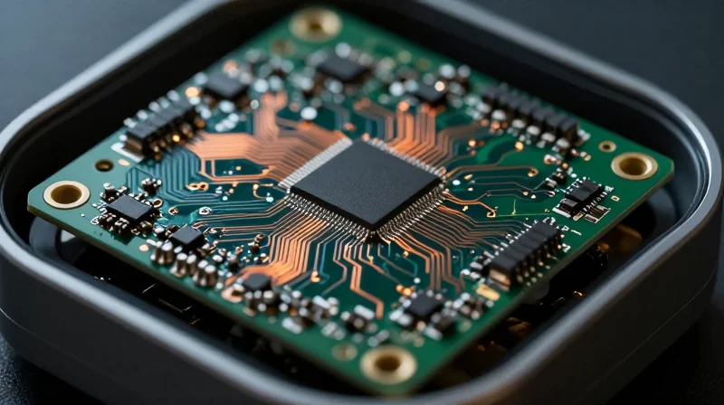
From Standard Multilayer to HDI Architectures
The evolution of wearable device engineering is defined by a relentless drive for smaller form factors without sacrificing computational density. Standard multilayer printed circuit boards (PCBs), while reliable for legacy consumer electronics, often reach a threshold where signal routing congestion and physical footprint limitations stifle innovation. The transition to High-Density Interconnect (HDI) technology represents a paradigm shift, enabling engineers to leverage microvias, blind and buried vias, and finer trace/space geometries to achieve unprecedented levels of integration within a confined spatial volume.
Comparative Analysis: Traditional vs. HDI Designs
| Feature | Standard Multilayer | HDI Architecture |
|---|---|---|
| Via Technology | Through-hole | Microvias (Laser-drilled) |
| Trace/Space Density | Conservative (>4 mil) | Aggressive (<3 mil) |
| Layer Count Efficiency | High footprint usage | Optimized high-density stacking |
| Component Placement | Limited by via footprint | Via-in-pad capability |
Key Drivers of HDI Adoption in Wearables
- Why is miniaturization the primary driver?
Wearables like smartwatches and medical patches require extreme battery-to-PCB volume ratios; HDI allows for smaller footprints, freeing up internal space for larger power cells or additional sensors. - How does signal integrity impact HDI selection?
As wearable devices integrate complex RF modules and high-speed processing, shorter interconnections provided by HDI architectures significantly reduce parasitic capacitance and inductance, enhancing overall system signal integrity. - Does HDI improve reliability in wearables?
By utilizing staggered or stacked microvia structures, engineers can maintain superior mechanical stability and structural integrity despite the reduction in board layers.
The successful adoption of HDI in wearables requires strict adherence to Design for Manufacturing (DFM) rules. Engineers must balance high-density requirements with fabrication constraints, such as aspect ratios for microvias and thermal management strategies, ensuring that the design remains manufacturable at scale without compromising yield.
Microvia Configuration Best Practices
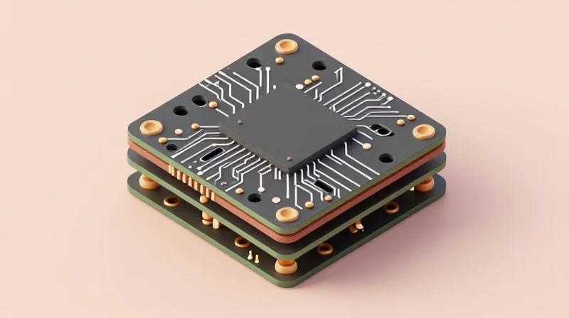
Microvia Geometry and Aspect Ratios
To ensure long-term reliability in wearable devices, microvia geometry must be tightly controlled. The industry standard dictates that the aspect ratio—the ratio of the hole depth to the hole diameter—should ideally not exceed 0.75:1 for reliable laser drilling and subsequent electrolytic copper filling. Exceeding a 1:1 ratio significantly increases the risk of 'dog-boning' and internal voids, which compromises structural integrity under thermal stress.
Landing Pad and Capture Requirements
The landing pad design is a critical factor in mitigating registration errors. For modern HDI boards, a 'capture' strategy is preferred over 'blind' landings wherever space permits.
| Feature | Recommended Design Constraint | Impact on Reliability |
|---|---|---|
| Minimum Pad Diameter | Hole Diameter + 150µm | Prevents breakout and improves registration tolerance |
| Via-in-Pad | Fully filled and capped (IPC-4761 Type VII) | Prevents solder wicking and ensures planar surface for assembly |
| Copper Wrap | Min 12µm thickness over hole shoulder | Reduces stress concentrations at the via transition |
Copper Wrap and Structural Integrity
Copper wrap, or the amount of copper extending from the via barrel onto the surface of the landing pad, is the primary defense against thermal fatigue. A robust copper wrap ensures that the transition between the via barrel and the trace is not a high-stress point. Designers should specify a minimum of 12µm of copper plating thickness to ensure the barrel-to-pad connection can withstand the CTE (Coefficient of Thermal Expansion) mismatch between the copper and the dielectric material during reflow cycles.
Frequently Asked Questions
- Can I use staggered microvias instead of stacked?
Yes, staggered microvias are generally more reliable as they distribute stress across multiple layers, though they may consume more board real estate. - Why is copper filling required for via-in-pad?
Filling and capping prevents solder from wicking into the via during assembly, which could otherwise create voids in the solder joint and cause premature electrical failure. - What is the maximum allowed copper plating void?
For HDI structures, the goal should be zero voids. Any voiding at the interface of the laser-drilled hole and the target pad will lead to accelerated electrochemical migration or cracking.
Optimizing Laser Drilling Parameters

Selecting the Laser Source: CO2 vs. UV
The choice between CO2 and UV laser systems is primarily dictated by the target material composition and the required via diameter. CO2 lasers excel at rapid ablation of dielectric layers but are limited in spot size, while UV lasers provide superior precision for sub-50µm vias.
| Feature | CO2 Laser | UV Laser (Nd:YAG) |
|---|---|---|
| Wavelength | 10.6 µm | 355 nm |
| Typical Via Size | Greater than 75 µm | 15 µm to 50 µm |
| Material Interaction | Thermal ablation of resin/glass | Photo-chemical breakdown |
| Best Application | High-throughput through-holes | Ultra-fine pitch HDI microvias |
Mitigating the Heat Affected Zone (HAZ)
Controlling the Heat Affected Zone (HAZ) is essential to prevent resin recession and micro-cracking in the dielectric. Excessive pulse energy leads to charring and copper delamination, compromising the reliability of subsequent plating processes.
- How does pulse energy affect hole quality?
Lower pulse energy increases processing time but significantly reduces carbonization and thermal shock, resulting in cleaner via walls ideal for high-reliability plating. - Why is glass weave a factor in HAZ management?
Laser energy absorption differs between resin and glass fiber. Using dual-laser processing—where a UV laser 'pre-cuts' the glass fibers—prevents uneven HAZ distribution caused by differential ablation rates. - What is the consequence of poor parameter optimization?
Sub-optimal parameters often lead to 'nail-heading' or ragged via walls, which significantly increase the risk of voiding during the chemical copper deposition process.
Mastering Blind-Via Aspect Ratios
The blind-via aspect ratio—defined as the ratio of hole depth to hole diameter—is the single most critical geometric constraint in HDI manufacturing. Because microvias are typically formed via laser ablation and metallized through electroplating, they present unique fluid dynamic challenges. As aspect ratios increase, the ability for plating chemistry to penetrate the full depth of the via diminishes, leading to 'voiding' or 'dog-boning' effects that compromise the long-term reliability of the device under thermal stress.
Standard Aspect Ratio Limits
| Via Type | Recommended Max Aspect Ratio | Critical Risk |
|---|---|---|
| Laser Drilled (Blind) | 0.75:1 to 1:1 | Incomplete plating coverage |
| Mechanical (Micro) | 0.5:1 | Plating solution entrapment |
| Stacked Blind Vias | 0.7:1 (cumulative) | Interlayer delamination |
Common Challenges in Via Metallization
- Why is 1:1 considered the upper bound?
Beyond a 1:1 ratio, the 'aspect ratio effect' creates a stagnant zone in the center of the via where ion transfer is severely restricted, leading to uneven copper deposition thickness. - How does surface finish affect aspect ratio viability?
Processes like Electroless Nickel Immersion Gold (ENIG) can become trapped in high-aspect-ratio vias, leading to corrosive residues that weaken the interconnect over time. - What is the impact of excessive Heat Affected Zone (HAZ) on plating?
If laser parameters are not optimized, the HAZ creates a rough dielectric wall surface, which increases the required plating thickness to achieve a smooth conductive layer, further reducing the effective diameter.
Engineering Recommendations for Wearables
To maintain structural integrity in high-density wearable designs, engineers should prioritize a 'shallow and wide' approach to microvia design. When board thickness necessitates a deeper via, consider utilizing staggered via configurations rather than stacked vias, as staggering improves thermal dissipation and reduces stress concentrations at the pad-to-via interface. Always consult with your fabrication partner early in the design phase, as their specific electroplating capabilities—such as pulse-reverse plating technology—can sometimes extend these aspect ratio limits slightly.
Preventing Common Fabrication Defects
Mitigating Delamination and Voids
Fabrication defects often stem from the coefficient of thermal expansion (CTE) mismatch between dielectric materials and copper interconnects. To prevent delamination, engineers must prioritize the selection of high-Tg (glass transition temperature) laminates that exhibit superior adhesion properties. Voiding within microvias is typically a result of inadequate desmear or poor wetting during the plating process; ensuring a standardized plasma desmear cycle is critical to removing resin residue and promoting uniform copper deposition.
Comparison of Common HDI Fabrication Defects
| Defect Type | Primary Root Cause | Prevention Strategy |
|---|---|---|
| Delamination | Excessive thermal shock during assembly | Utilize high-Tg materials; improve moisture pre-baking |
| Via Voiding | Incomplete desmear; entrapped air | Optimize plasma power; ensure electrolyte flow |
| Etch-back/Smear | Improper drilling pulse energy | Calibrate laser frequency; refine desmear duration |
Troubleshooting Drilling and Plating Challenges
- How does laser pulse frequency impact hole-wall quality?
Excessive pulse energy creates a large Heat Affected Zone (HAZ), leading to carbonized resin residue. Maintaining precise energy settings per dielectric thickness is essential for a clean via barrel. - What role does surface tension play in microvia plating?
In high-aspect-ratio blind vias, electrolyte circulation is restricted. Using pulsed reverse plating (PRP) techniques facilitates better ion exchange, significantly reducing the occurrence of plating voids. - Can improper storage lead to fabrication failure?
Yes. HDI structures are highly susceptible to moisture absorption. Implementing strict vacuum-sealed storage protocols is necessary to prevent 'popcorning' or delamination during reflow.
Ultimately, the stability of an HDI PCB rests on the synergy between precise laser drilling and chemical plating efficiency. By standardizing these parameters through DFM guidelines, designers can drastically reduce the scrap rate and enhance the operational lifespan of miniaturized wearable devices.
Strategic Stack-Up Design for Signal Integrity
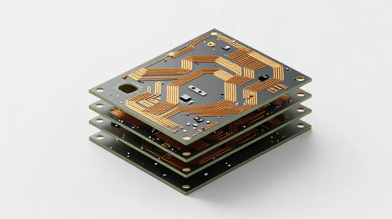
Balancing Signal Integrity and Thermal Management
Designing a high-density interconnect (HDI) stack-up for wearables requires a dual-track strategy: maintaining precise impedance control while providing sufficient heat dissipation paths. As signal frequencies increase, trace geometry and dielectric selection become critical, while the compact nature of wearables necessitates effective thermal management to avoid performance throttling.
| Design Factor | Signal Integrity Strategy | Thermal Management Strategy |
|---|---|---|
| Copper Pour | Reference plane continuity | Increased surface area for heat sinking |
| Via Placement | Minimizing return path impedance | Utilizing thermal vias to internal planes |
| Dielectric Choice | Low-loss tangent (Df) materials | Higher thermal conductivity (Tg) |
Critical Guidelines for Stack-Up Optimization
- How does reference plane selection affect high-speed signals?
Using a solid, unbroken reference plane directly adjacent to signal layers is mandatory to minimize loop inductance and provide a predictable return path, which prevents EMI radiation. - Can thermal vias negatively impact signal integrity?
If not properly controlled, high-density thermal via arrays can cause impedance discontinuities due to excessive capacitive loading; stagger them appropriately or use microvias to mitigate this. - What is the role of the dielectric in wearable HDI?
Thin core materials reduce overall height, but must be chosen for a low dielectric constant (Dk) and low dissipation factor (Df) to maintain signal speed and reduce power loss.
Implementing Controlled Impedance
To achieve reliable impedance control in thin HDI structures, designers must account for copper roughness and resin content variability. Utilizing laser direct imaging (LDI) and strict manufacturing tolerances for trace width ensures that signal integrity remains consistent across production batches, even as board thickness shrinks to sub-0.5mm levels.
Streamlining the Prototyping to Production Workflow

Harmonizing DRC with Fab Capabilities
The primary cause of delays in wearable PCB development is the discrepancy between internal Design Rule Checks (DRC) and the specific limitations of the fabrication facility. To streamline the workflow, engineers must integrate vendor-specific constraint files directly into their CAD environment. This proactive alignment prevents 'black-box' rejections at the pre-production stage, ensuring that design intent is inherently manufacturable.
Key Strategic Alignment Metrics
| Parameter | Prototype Focus | Production Optimization |
|---|---|---|
| Via Geometry | Laser ablation flexibility | Standardized aspect ratios |
| Trace/Space | Advanced patterning | Reliable copper weight uniformity |
| Panelization | Individual coupons | High-density array utilization |
Accelerating Time-to-Market
Transitioning from a functional prototype to a mass-produced wearable requires a shift from 'performance-first' to 'reliability-first' design. By implementing a concurrent engineering approach—where the fabricator provides feedback on panel layout and copper balancing during the design phase—teams can reduce cycle times by up to 30%.
- How does early vendor engagement affect prototype speed?
Early engagement allows for the adjustment of stack-up and material selection to match the fabricator's current stock, avoiding long-lead-time material sourcing issues. - Why is 'Design for Manufacture' (DFM) verification critical before data release?
Automated DFM verification identifies potential plating voids and etching inconsistencies that are often overlooked by standard DRC, preventing costly re-spins. - What role does panelization play in production efficiency?
Optimizing panel utilization reduces waste and ensures uniform thermal distribution during the lamination process, which is critical for thin HDI boards.
Mastering these HDI DFM rules is essential for scaling your production without compromising reliability. By optimizing your microvia and laser drilling strategy now, you mitigate costly redesigns and fabrication delays. Ready to elevate your PCB manufacturing standards? Contact our engineering team today to review your current design files for DFM optimization.
