
In the competitive landscape of modern electronics, product miniaturization isn't just an aesthetic choice—it's a critical performance lever. As device footprints shrink and power requirements intensify, traditional board design often hits a wall. In this article, we break down a real-world case study revealing how strategic investments in High-Density Interconnect (HDI) technology not only optimize board real estate but serve as a catalyst for superior energy efficiency and long-term cost savings.
The Evolution of PCB Density: Why HDI is the New Standard
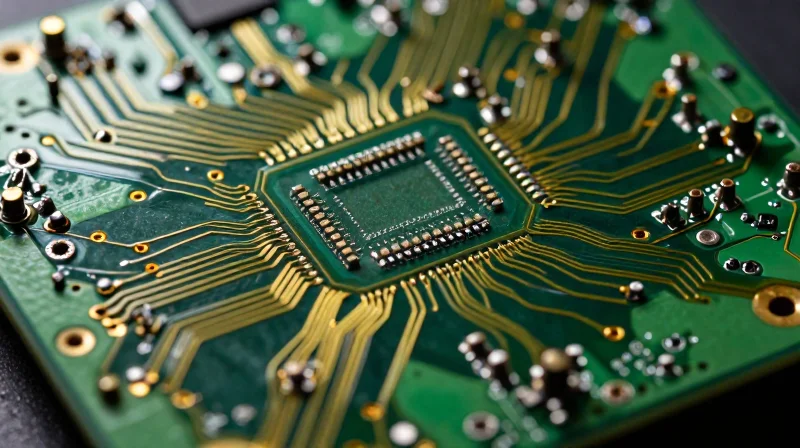
From Multilayer to HDI: The Paradigm Shift
For decades, standard multilayer printed circuit boards (PCBs) served as the backbone of electronic engineering. However, the rise of wearable technology and compact mobile devices has pushed these traditional fabrication methods to their physical limits. Conventional boards rely on through-hole vias that penetrate every layer, consuming valuable routing space and limiting component density. HDI technology solves this by employing microvias—laser-drilled structures that only span between adjacent layers—drastically opening up inner-layer routing capacity.
Comparing PCB Fabrication Technologies
| Feature | Conventional Multilayer | HDI Technology |
|---|---|---|
| Via Structure | Through-hole | Microvia (Blind/Buried) |
| Component Density | Low to Moderate | Ultra-High |
| Signal Integrity | Limited by stub length | Excellent (minimal stubs) |
| Routing Complexity | High layer count required | Reduced layer count |
Key Drivers of the HDI Standard
The industry's move toward HDI is not merely a design preference; it is a necessity driven by the requirements of modern IC packages. Smaller pads and finer line widths are essential to accommodate Ball Grid Array (BGA) components with tighter pin pitches. By reducing the reliance on large through-holes, designers can utilize thinner dielectrics and closer routing paths, directly contributing to smaller form factors.
- How do microvias improve battery life?
Microvias reduce the electrical path length and parasitic capacitance. This improved signal efficiency consumes less power during data transmission, directly extending the operational runtime of wearable devices. - Why does HDI reduce production costs?
While unit costs can appear higher, HDI reduces overall PCB surface area and layer counts. This allows for more units per panel during fabrication, lowering the per-board manufacturing cost while enabling more feature-rich, high-value devices. - Is HDI reliable for consumer wearables?
Yes. HDI structures offer superior thermal management and reduced mechanical stress on components, ensuring durability in compact environments where vibration and temperature fluctuations are common.
Case Study: Redesigning for High-Density Interconnects
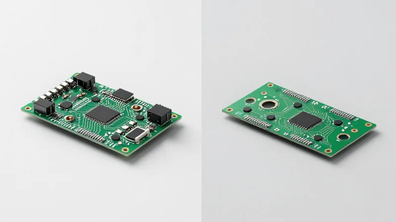
Transitioning to HDI: The Engineering Challenge
A leading wearable technology manufacturer recently faced a critical bottleneck: their legacy 8-layer rigid board was limiting the product's footprint, forcing a compromise on battery volume. By migrating to a 2-4-2 HDI stackup utilizing laser-drilled microvias, the engineering team was able to shrink the total board area by 35% while increasing signal routing density.
| Metric | Legacy Multilayer | Optimized HDI Design |
|---|---|---|
| Board Footprint | 4200 mm² | 2730 mm² |
| Layer Count | 8-Layer Through-Hole | 2-4-2 HDI Stackup |
| Via Type | Mechanical Drill | Laser-Drilled Microvia |
| Battery Capacity | 280 mAh | 345 mAh |
Impact on Production Costs and ROI
While HDI manufacturing requires a higher initial investment in fabrication technology, the transition yielded a net cost reduction. The reduced board size allowed for a higher yield per panel during fabrication, and the simplified routing significantly decreased the scrap rate caused by signal interference and thermal management issues inherent in the older design.
- How did HDI improve battery life?
By reclaiming internal board space via microvias, the design allowed for a larger physical battery cell, resulting in a 23% increase in total energy capacity. - What was the primary driver of cost savings?
The primary drivers were increased panel utilization efficiency and lower assembly rework rates due to the improved integrity of signal paths and reduced layer complexity. - Was the design cycle longer?
Initially yes, due to the need for advanced simulation, but the long-term ROI was realized through reduced product returns and faster product iteration cycles.
Technical Takeaway
The successful migration proves that HDI is not merely a density play; it is an economic strategy. By consolidating board layers, engineers can simultaneously lower material costs, reduce power consumption through shorter traces, and increase the value proposition of the final wearable product.
Reducing Total Cost of Ownership Through Material Efficiency
Optimizing Substrate Footprint and Layer Counts
The primary driver of cost reduction in HDI implementation is the strategic consolidation of board real estate. By utilizing microvias—specifically laser-drilled blind and buried vias—designers can route signals more efficiently, often reducing the total layer count required to achieve the same functionality as a conventional multilayer board. Smaller boards require less laminate and copper foil, directly decreasing the raw material costs per panel. Furthermore, because more boards fit onto a single standard manufacturing panel, the unit cost is effectively reduced through higher yield density.
Manufacturing Efficiency and Processing Time
| Metric | Conventional Multilayer | Optimized HDI Design |
|---|---|---|
| Board Area | Baseline | 20-40% Reduction |
| Layer Count | Standard (e.g., 10-12) | Aggressive (e.g., 6-8) |
| Panel Yield | Baseline | 30-50% Increase |
| Processing Time | High (More drill cycles) | Low (Simplified routing) |
Processing efficiency represents a hidden savings opportunity. HDI manufacturing reduces the total drill hits required for through-hole vias, replacing them with precision laser processes that are faster and less prone to registration errors. This reduction in complex drilling cycles minimizes the risk of manufacturing defects, thereby increasing production yields and decreasing the necessity for costly rework or scrap, which are significant contributors to the overall total cost of ownership (TCO).
Frequently Asked Questions
- Does HDI increase per-unit fabrication costs?
While the per-layer cost of HDI is higher, the total system cost is often lower due to significant reductions in board size and material volume. - How does HDI impact assembly labor?
Advanced HDI boards facilitate smaller, more compact component placement, which can streamline SMT (Surface Mount Technology) assembly cycles and reduce overall housing costs for wearable devices. - Is the transition to HDI worth the initial engineering investment?
Yes, for high-volume wearables, the initial NRE (Non-Recurring Engineering) cost is rapidly amortized through lower unit costs and improved device performance metrics like battery longevity.
The Direct Link Between HDI Design and Battery Efficiency
Optimizing Signal Paths and Power Efficiency
The transition to High-Density Interconnect (HDI) technology is not merely a method for miniaturization; it is a fundamental engineering strategy for power management. By utilizing laser-drilled microvias and finer conductor geometries, designers can drastically shorten the physical length of traces between the MCU, sensors, and power management ICs. This reduction in trace length directly translates to lower parasitic resistance, minimizing voltage drops and ohmic heating that would otherwise deplete a battery's energy reserve.
Comparative Impact of Design Methodologies
| Design Factor | Standard PCB Performance | Optimized HDI Performance |
|---|---|---|
| Average Trace Length | Long (Higher Resistance) | Short (Lower Resistance) |
| Parasitic Capacitance | High (Signal Loading) | Low (Faster Switching) |
| Power Consumption | Higher I2R Losses | Minimized Energy Loss |
Technical Advantages in Battery Longevity
Beyond resistance, HDI architectures allow for superior signal integrity by facilitating tighter ground plane coupling and reducing loop area. This reduction in loop area is critical for minimizing EMI, which reduces the need for power-hungry filtering components. When the signal environment is inherently cleaner, the system can operate at lower voltage thresholds without sacrificing reliability, directly extending the time between battery recharge cycles.
- How does shorter trace length impact battery life?
Shorter traces reduce total copper resistance, which lowers I2R power dissipation, ensuring that more energy is delivered to the load rather than being lost as heat. - Why do microvias improve energy efficiency?
Microvias eliminate long, indirect via stubs that act as antennas and capacitive loads, allowing for cleaner high-speed signal propagation and reduced switching power demands. - Is HDI design cost-effective for power saving?
While initial design complexity is higher, the ROI is realized through increased battery density, improved market competitiveness, and reduced component count for power regulation.
Overcoming Manufacturing Challenges with HDI
Addressing Fabrication and Reliability Constraints
Transitioning to HDI designs often raises concerns regarding via reliability and thermal management. By moving from mechanical to laser-drilled microvias, engineers can achieve greater density without compromising the structural integrity of the substrate. Advanced sequential lamination processes allow for tighter tolerances, effectively neutralizing the risks typically associated with miniaturized interconnects while simultaneously improving signal path consistency.
| Challenge | HDI Mitigation Strategy | Impact on Production |
|---|---|---|
| Registration Accuracy | Advanced LDI Imaging | Higher Yield Rates |
| Via Reliability | Copper-Filled Microvias | Enhanced Thermal Stability |
| Signal Integrity | Optimized Stack-up Design | Reduced Re-spin Requirements |
Frequently Asked Questions Regarding HDI Implementation
- Does higher density increase the risk of thermal failure?
No; by utilizing copper-filled microvias and optimized ground planes, HDI designs offer superior heat dissipation pathways compared to traditional through-hole technology. - How can teams minimize the cost of HDI fabrication?
Prioritizing standardized via structures and minimizing the number of lamination cycles significantly reduces fabrication complexity and associated overhead costs. - Is HDI reliability proven for high-vibration wearable environments?
Yes, laser-formed microvias provide a smaller, more robust connection point that is less susceptible to mechanical stress and fatigue than standard through-hole vias.
Market Longevity: Future-Proofing Your Hardware
The Architectural Advantage of HDI for Future-Proofing
Future-proofing wearable hardware is not simply about over-engineering current specifications; it is about establishing a scalable design foundation that can absorb future feature integration without necessitating a complete board redesign. HDI (High Density Interconnect) technology provides the essential modularity required to sustain growth. By utilizing microvias and finer line widths, engineers can compress existing circuitry, leaving valuable 'real estate' on the PCB for future sensors, improved antennas, or expanded memory modules.
Comparing Design Strategies for Product Evolution
| Design Factor | Legacy Multilayer PCB | Advanced HDI PCB |
|---|---|---|
| Scalability | Low (Rigid structure) | High (Flexible routing) |
| Integration Capacity | Limited | Excellent for future silicon |
| Signal Path Optimization | Fixed | Dynamic/Shortened |
| Component Density | Low | High (Up to 40% reduction) |
Strategic Longevity Through Signal Integrity
As wearable devices transition toward 5G connectivity and edge-AI processing, the demands on signal integrity become exponentially more stringent. HDI design naturally minimizes parasitic capacitance and inductance by reducing trace length and complexity. This performance buffer ensures that when next-generation processors with higher clock speeds are introduced into a product line, the underlying PCB substrate is already capable of supporting the increased bandwidth and tighter timing margins without degradation.
Frequently Asked Questions
- Does switching to HDI increase upfront design costs?
While initial design complexity is higher, HDI reduces long-term costs by extending the product lifecycle, allowing for iterative hardware updates on the same board platform rather than frequent ground-up redesigns. - How does HDI help with future feature creep?
By optimizing routing and utilizing buried/blind vias, HDI recovers PCB surface area. This space serves as a buffer, enabling engineers to add components like biometric sensors or improved NFC modules in subsequent versions without expanding the device form factor. - Can HDI designs handle the heat of future processors?
Yes, through advanced thermal management via patterns and improved layer stacking, HDI facilitates better heat dissipation, ensuring that higher-performance future chips can operate within the thermal envelope of current chassis designs.
Best Practices for Implementing HDI in Your Next Product
Transitioning to High-Density Interconnect (HDI) technology is a pivotal move for wearable product teams, yet it demands a departure from traditional rigid-flex or standard multilayer design methodologies. To maximize ROI and ensure battery longevity, teams must synchronize their CAD environments with manufacturing capabilities early in the development lifecycle.
Strategic Implementation Checklist
- Early Manufacturer Engagement
Consult your fabrication partner during the schematic phase to align your stack-up constraints with their laser-via drilling capabilities and plating process limitations. - Via Structure Selection
Prioritize micro-via-in-pad structures to reduce trace lengths, effectively minimizing parasitic inductance and lowering power consumption for extended battery life. - Stack-up Optimization
Utilize sequential lamination processes carefully; while they increase density, they also add cost, so focus on utilizing only the necessary layer counts to balance complexity with price-per-unit. - Design Rule Checks (DRC)
Automate your DRC settings to handle advanced HDI constraints, specifically focusing on aspect ratios for micro-vias and minimal copper-to-copper clearances.
HDI Design Comparison: Traditional vs. HDI
| Feature | Traditional PCB | Advanced HDI |
|---|---|---|
| Via Technology | Through-hole | Laser Micro-via |
| Routing Density | Low/Medium | Ultra-High |
| Signal Integrity | Moderate Parasitics | Minimal Noise/Latency |
| Manufacturing Cost | Baseline | Premium (Offset by miniaturization) |
Optimizing for Wearable Power Profiles
Beyond the physical layout, HDI offers an intrinsic advantage in power delivery. By shortening the physical distance between power management integrated circuits (PMICs) and high-speed processors, you reduce IR drop and heat dissipation. When implementing your next product, prioritize 'power-first' placement within your HDI routing strategy to squeeze every milliampere-hour out of your wearable’s battery.
By moving beyond legacy PCB designs and embracing the precision of HDI technology, organizations can unlock unprecedented levels of power efficiency and cost-effectiveness. As showcased in our case study, these investments pay dividends in both product performance and long-term market viability. Are you ready to optimize your device's architecture? Contact our engineering team today for a custom assessment of your next high-density design project.
