
In the fast-paced world of wearable fitness technology, device failure isn't just an inconvenience—it’s a brand-killing event. As designs shrink, the complexity of High-Density Interconnect (HDI) boards rises, demanding a manufacturing partner who understands both precision and longevity. This guide breaks down the essential criteria for selecting a PCB partner that turns your innovative concepts into market-ready, high-performance wearables.
Evaluating HDI Technical Proficiency
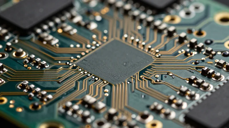
Assessing Micro-via and Interconnect Capabilities
High-performance fitness trackers rely on High-Density Interconnect (HDI) structures that utilize complex micro-via architectures to conserve board space. When vetting a partner, you must verify their proficiency in laser drilling blind and buried vias, as inconsistent depth control can lead to catastrophic signal failures. Look for evidence of stacked and staggered via reliability testing, as these techniques are fundamental to routing high-density BGA packages in miniature form factors.
Technical Competency Comparison
| Capability | Performance Requirement | Manufacturer Metric |
|---|---|---|
| Laser Micro-via | High density integration | Aspect ratio accuracy |
| Fine Pitch (BGA) | Complex routing | Pad-in-Via feasibility |
| Registration | Signal integrity | Layer-to-layer tolerance |
Frequently Asked Questions on HDI Manufacturing
- What is the primary risk of choosing a manufacturer without advanced HDI experience?
Without specialized HDI expertise, manufacturers often struggle with registration accuracy, leading to open circuits or intermittent connectivity in dense multi-layer stacks common in wearables. - How do you verify a manufacturer's ability to handle fine-pitch components?
Request their DFM (Design for Manufacturing) guidelines and ask for specific examples of successful runs involving 0.4mm or finer BGA pitches, including their minimum trace/space capability. - Why is copper plating quality critical for micro-vias?
Uniform copper distribution within micro-vias is essential to prevent thermal stress fractures, which are frequent failure points in wearable devices subjected to constant movement and temperature cycling.
The Significance of IPC Class 3 Standards
Defining IPC Class 3 for Wearable Electronics
IPC Class 3 represents the highest tier of printed circuit board manufacturing, designated for 'High-Performance Electronic Products' where continued performance or performance-on-demand is critical. In the context of wearable fitness trackers, this means the device must function reliably in harsh, unpredictable environments, such as during intense exercise involving moisture, thermal cycling, and physical impact. Choosing a manufacturer that adheres to IPC Class 3 guarantees tighter tolerances in drilling, plating, and etching that standard consumer-grade production often overlooks.
Class 2 vs. Class 3: Key Reliability Distinctions
| Feature | IPC Class 2 (Standard) | IPC Class 3 (High-Reliability) |
|---|---|---|
| Plating Thickness | Minimum 20µm | Minimum 25µm |
| Annular Ring | Reduced allowed | Stricter requirements |
| Inspection Criteria | Standard AQL | Enhanced/Visual focus |
| Application | General electronics | Medical/Mission-critical |
Why Class 3 is Non-Negotiable for Wearables
- Why does moisture resistance matter?
Class 3 manufacturing processes ensure better copper plating in vias, which prevents micro-cracks and subsequent short circuits caused by sweat and humidity ingress. - How does it affect device lifespan?
Wearables face constant thermal cycling as the body heats up and the device cools down; Class 3 adherence minimizes fatigue at solder joints and via barrels. - Is Class 3 worth the higher cost?
While unit costs are higher, the reduction in field failures and warranty claims in medical-grade fitness tracking makes it a cost-effective long-term strategy for high-performance brands.
When selecting an HDI PCB partner, verify their certifications and request to see their quality assurance logs. A manufacturer fully integrated with IPC Class 3 standards will provide transparent documentation of their process controls, ensuring that your high-performance wearable maintains its integrity under the most demanding conditions.
Optimizing Layer Stack-Up for Form Factor
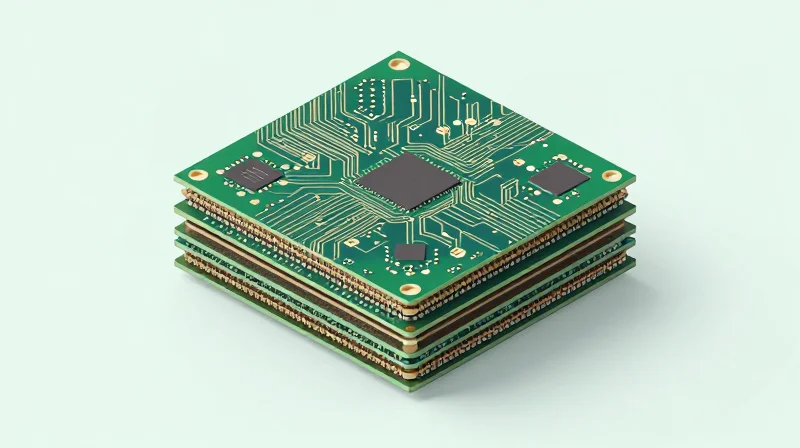
In the context of wearable fitness trackers, the PCB stack-up serves as the foundation for both mechanical footprint reduction and electrical performance. Achieving a compact form factor requires a strategic approach to layer count, material selection, and micro-via utilization, ensuring that the design remains manufacturable while meeting the high-density interconnect (HDI) requirements of modern wearable SoCs.
Balancing Density with Thermal Performance
Engineers often face a trade-off between increasing layer count to save board area and managing the thermal dissipation of high-performance components. Effective HDI stack-up design leverages thin, low-loss dielectric materials and carefully placed thermal vias. Selecting a manufacturing partner capable of processing high-Tg (glass transition temperature) materials is vital to ensure the board withstands the repeated thermal cycling inherent in fitness-tracking environments.
| Parameter | Standard Design | Optimized Wearable Design |
|---|---|---|
| Via Technology | Through-hole | Stacked/Staggered Micro-vias |
| Core Thickness | 10-12 mil | 2-4 mil |
| Signal Integrity | Standard FR4 | High-Frequency/Low-Loss Laminates |
| Thermal Management | Heat Spreader | Thermal Vias/Plane Copper Pour |
Technical Considerations for HDI Stacking
- How does via-in-pad technology impact the form factor?
Via-in-pad allows components to be placed directly over vias, significantly reducing the footprint and signal path length, which is crucial for the extreme density of fitness wearables. - Why is layer symmetry important in HDI stacks?
Symmetrical layer stacking prevents PCB warping during the lamination and reflow process, a common failure point when using thin, high-layer-count substrates. - How do you ensure signal integrity in thin stacks?
By utilizing controlled impedance routing and minimizing the distance between signal layers and reference ground planes, you mitigate crosstalk and EMI issues.
Advanced Material Selection for Durability

Advanced Material Selection for Durability
Wearable devices exist in uniquely hostile environments. Unlike static electronics, fitness trackers face constant exposure to human perspiration, which is chemically corrosive, alongside rapid thermal cycling and repeated mechanical shock. Selecting the right base material—specifically high-glass transition temperature (high-Tg) laminates and low-loss dielectrics—is the primary defense against board delamination and signal degradation.
Material Performance Matrix
| Material Property | Standard FR-4 | High-Performance HDI Substrate |
|---|---|---|
| Tg (Glass Transition Temp) | ~130-140°C | 170°C - 180°C+ |
| Moisture Absorption | High (prone to CAF) | Ultra-low (moisture resistant) |
| Thermal Shock Resistance | Low | Excellent (via integrity) |
| Signal Loss (Df) | Higher | Low/Ultra-Low |
Key Considerations for Durability
- Mitigating Conductive Anodic Filament (CAF) Growth
Choose materials specifically engineered for CAF resistance to prevent electrical shorts caused by moisture wicking along glass fiber bundles, a common failure point in sweaty environments. - Thermal Expansion Matching
Ensure the coefficient of thermal expansion (CTE) of the dielectric matches the copper layers to minimize stress on micro-vias during the rapid heat cycling common in high-intensity workouts. - Halogen-Free Compliance
Prioritize halogen-free laminates that offer superior flame retardancy without sacrificing the mechanical rigidity required to withstand accidental drops and impacts.
When auditing an HDI manufacturer, request their material qualification data specifically for high-density, multi-layer applications. A partner worth considering will provide detailed reports on how their chosen resin systems hold up against aggressive environmental testing, including humidity chamber cycling and vibration analysis.
DFM Review and Pre-Manufacturing Support
The Role of Proactive DFM in HDI Design
Design for Manufacturing (DFM) is not merely a final checklist; it is an essential engineering collaboration that ensures your HDI PCB design is optimized for the specific processes of your selected manufacturer. By performing a comprehensive DFM review early in the development cycle, engineers can resolve issues related to drill-to-copper clearances, via-in-pad geometry, and solder mask registration, preventing expensive post-design layout modifications.
Common HDI Fabrication Risks
| Risk Factor | Impact on Performance | Mitigation Strategy |
|---|---|---|
| Via-in-Pad Voiding | Open circuits or intermittent failure | Implement specific conductive/non-conductive epoxy filling |
| Aspect Ratio Violations | Plating failure in high-aspect holes | Adjust board thickness or drill diameter via DFM feedback |
| Copper Weight Inconsistency | Impedance mismatch in high-speed lines | Ensure uniform copper distribution during stack-up design |
Collaborative Pre-Manufacturing Support
The best manufacturers treat DFM as a partnership rather than an adversarial review process. An elite HDI shop will offer pre-manufacturing support that includes impedance modeling, thermal profiling, and panelization optimization to increase yield while maintaining structural integrity in ultra-thin wearables.
- Why should I submit my design for a DFM review before final tape-out?
Early review identifies manufacturing constraints, such as trace width limits or plating challenges, that would otherwise cause production stops or yield losses. - How does panelization improve my project cost?
Optimizing panel layout maximizes the number of boards produced per substrate sheet, significantly reducing the cost per unit while improving fabrication efficiency. - What documentation should I expect from the manufacturer post-review?
You should receive a detailed DFM report highlighting recommended adjustments to layer stack-up, design rules, and potential areas of concern that may affect reliability.
Supply Chain Transparency and Quality Assurance
Ensuring End-to-End Supply Chain Transparency
In the fast-paced wearable market, supply chain transparency is not just an administrative requirement; it is a critical safeguard against counterfeit components and substandard materials. High-performance fitness trackers rely on high-density interconnect (HDI) boards that utilize specific resin systems and ultra-thin glass weaves. An ideal manufacturing partner must provide full visibility into their sourcing pipeline, proving that all raw materials are sourced from reputable, audited suppliers who comply with RoHS, REACH, and conflict-free mineral standards.
Rigorous Traceability and Batch Consistency
Maintaining consistency across high-volume production runs requires granular traceability. Manufacturers must implement a robust serialization strategy, where each PCB panel is tracked from the raw laminate stage through chemical etching and final inspection. This level of oversight ensures that if a field failure occurs, the manufacturer can immediately identify the specific production batch, facility, and time window associated with that board, facilitating rapid root-cause analysis.
| Feature | Requirement for Wearables | Impact of Failure |
|---|---|---|
| Material Lot Tracking | Full lot numbers on all laminates/pre-pregs | Unidentified board delamination |
| Process Auditing | ISO 9001, IATF 16949, ISO 13485 | Inconsistent signal integrity performance |
| Verification | Automated Optical Inspection (AOI) | Latent micro-shorts in HDI vias |
Quality Assurance FAQ
- How do I verify the manufacturer's quality management system?
Always request current, valid copies of ISO certifications. For wearables, prioritize partners who hold ISO 13485, as it mirrors the strict quality management requirements necessary for consumer health electronics. - What testing methods ensure long-term wearable durability?
Look for manufacturers that provide Thermal Shock Testing and Highly Accelerated Life Testing (HALT). These protocols mimic the stress caused by skin contact, sweat exposure, and movement cycles inherent in fitness tracking. - Why is material batch consistency critical for HDI?
HDI designs utilize tightly coupled layer stacks. Even minor variations in the dielectric constant (Dk) or dissipation factor (Df) of the substrate between different material batches can lead to impedance mismatches and signal loss.
Prototyping to Mass Production Scalability
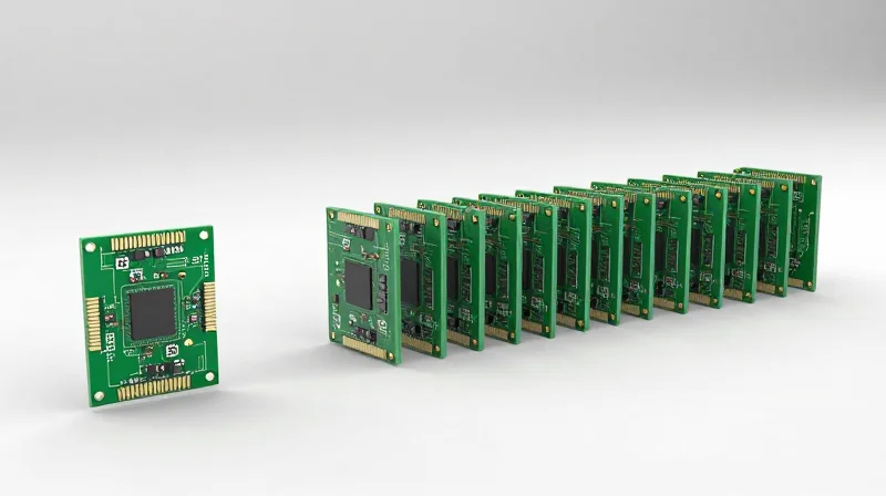
Bridging the Prototype-to-Production Gap
The greatest risk in high-performance wearable development is a 'manufacturing cliff' where a prototype designed on experimental processes fails to translate to mass-production line speeds. A competent HDI manufacturer bridges this gap by utilizing scalable equipment platforms—such as laser direct imaging (LDI) and automated optical inspection (AOI) systems—that maintain performance characteristics across varying volumes.
| Feature | Prototyping Phase | Mass Production Phase |
|---|---|---|
| Tooling | Soft tools/digital imaging | Hard tooling/automated jigs |
| Panel Size | Small or partial panels | Optimized standard panels |
| Yield Focus | Design verification | Process stability and cost |
Key Considerations for Scalable HDI Manufacturing
- Is the manufacturer equipment-agnostic?
Ensure they use the same core HDI process (e.g., sequential build-up) for prototypes as they do for production runs to prevent unexpected signal integrity shifts. - What is their panelization strategy?
Early collaboration on board panelization ensures optimal material utilization, which dramatically lowers unit costs as production ramps up from hundreds to millions of units. - How is design portability managed?
A top-tier partner maintains a digital thread, ensuring that design tweaks made during prototyping are automatically updated in the fabrication CAM files used for full-scale production.
Ensuring Reliability at Scale
Scaling production for fitness trackers involves strict statistical process control (SPC). Beyond simple functionality, your manufacturer must demonstrate long-term reliability through consistent testing of via plating thickness, dielectric adhesion, and thermal cycling. Verify that their cleanroom environment and automated sorting processes remain consistent regardless of order volume, ensuring that every wearable device shipped meets the rigorous endurance standards required for fitness-centric hardware.
Cost vs. Value: Protecting Your ROI
The Hidden Costs of Low-Bid Manufacturing
In the high-performance wearable market, selecting a manufacturer based solely on the lowest per-unit quote is a dangerous strategy. For HDI PCBs, where microvias and thin laminates are standard, a cheap quote often reflects cut corners in material quality, drilling precision, or inspection depth. These shortcuts inevitably manifest as high field failure rates, degraded battery life, or complete device bricking, which can destroy your brand reputation far more quickly than a slightly higher upfront component cost.
| Cost Factor | Low-Bid Manufacturer Impact | Value-Driven Manufacturer Impact |
|---|---|---|
| Material Quality | Substandard Tg laminates prone to thermal fatigue | High-performance materials ensuring long-term reliability |
| Yield Rates | Frequent scrap and mid-production delays | High first-pass yield and consistent throughput |
| Field Returns | High risk due to latent defects | Minimal risk with rigorous stress testing |
Protecting Your Return on Investment
Protecting your ROI requires a shift from viewing the PCB as a commodity to treating it as a core performance asset. A strategic partner adds value by offering pre-emptive failure analysis and high-fidelity testing, which drastically reduces the costs associated with post-deployment remediation.
- Does a lower price ever justify higher risk?
For wearable fitness trackers, which face constant physical movement and sweat exposure, the cost of a single recall far outweighs the savings of a cheaper PCB. Prioritizing reliability is the only way to preserve long-term margins. - How can I quantify the value of an experienced partner?
Evaluate the manufacturer based on their 'Total Landed Quality,' which includes their ability to provide comprehensive test reports, material traceability, and proactive engineering support that prevents costly redesigns. - What should I look for in a quote besides price?
Look for explicit mentions of inspection standards (IPC-Class 3), validation of HDI build-up techniques, and the inclusion of post-fabrication reliability testing protocols in your quote.
Selecting an HDI PCB manufacturer is about more than just matching quotes; it is about finding a partner committed to the engineering excellence required for next-gen wearables. By prioritizing technical rigor, material quality, and design collaboration, you can protect your device’s reputation and ensure a smooth path to production. Ready to take your wearable design to the next level? Contact our engineering team today to discuss your next high-performance project.
