
In the world of high-speed electronics, the margin for error in signal integrity is razor-thin. As edge rates increase, your PCB stack-up is no longer just a physical support structure; it is a critical transmission line component. This guide explores the essential Design for Manufacturing (DFM) rules required to ensure your impedance-controlled designs survive the transition from CAD to fabrication without compromising signal performance.
Understanding the Fundamentals of Impedance Control

The Essence of Controlled Impedance
Controlled impedance refers to the precise matching of PCB trace geometry and dielectric properties to maintain a constant characteristic impedance throughout the signal path. In high-speed design, a transmission line is not merely a copper wire but a wave-guiding structure; when the impedance changes abruptly, a portion of the electromagnetic energy is reflected back toward the source, causing signal degradation, ringing, and increased electromagnetic interference (EMI).
Why Impedance Control is Non-Negotiable
As edge rates decrease (faster switching speeds), the wavelength of the signal becomes comparable to the length of the traces. At these frequencies, transmission line effects dominate. Controlled impedance ensures that the energy propagating down the trace encounters a uniform environment, effectively preventing signal reflections that would otherwise corrupt the bitstream and compromise data integrity.
| Feature | Controlled Impedance | Uncontrolled Impedance |
|---|---|---|
| Signal Integrity | Maintains clean wave propagation | Susceptible to reflections and noise |
| High-Speed Capability | Essential for multi-GHz signals | Limited to low-speed or DC |
| EMI Performance | Low emission, stable return path | High emission, resonant loops |
Key Impedance Parameters
- Trace Width
A primary geometric variable; increasing width decreases impedance. - Dielectric Height
The distance between the trace and the reference plane; increasing the height increases impedance. - Dielectric Constant (Dk)
The material property affecting wave propagation speed; a higher Dk lowers impedance. - Copper Thickness
Influences the side profile and cross-sectional area; thicker copper decreases impedance slightly.
The Role of Dielectric Constant (Dk) in Material Selection
The Physics of Dk and Impedance
The dielectric constant, or relative permittivity (Er), measures a material's ability to store electrical energy in an electric field. In impedance-controlled PCB design, Dk is a foundational variable in the transmission line equation. Because signal propagation velocity is inversely proportional to the square root of the effective Dk, even minor variations in material composition across a substrate can lead to phase shifts, timing jitter, and impedance discontinuities.
Impact of Dk Variations on Signal Integrity
| Parameter | Effect of High Dk | Effect of Low Dk |
|---|---|---|
| Propagation Delay | Increased (Slower signals) | Decreased (Faster signals) |
| Trace Width | Requires narrower traces for 50 Ohm | Allows wider traces for 50 Ohm |
| Field Confinement | Higher crosstalk potential | Better isolation |
Engineering for Consistency: The Fabricator Partnership
Dielectric constants are not static; they fluctuate with frequency, temperature, and moisture absorption. Engineers must treat Dk as a dynamic parameter. Collaborating with your fabricator is essential because they possess real-world 'fabrication-specific' Dk values (often slightly different from datasheet nominals) based on their specific lamination process, copper weight, and resin flow.
- Why is the nominal Dk from a datasheet often insufficient?
Datasheet values are typically measured at 1 MHz, whereas high-speed signals operate at GHz frequencies. Material properties change significantly at higher frequencies, requiring the use of 'design-frequency Dk' values provided by your supplier. - What is the danger of using 'glass weave effect' in calculations?
Woven fiberglass substrates create localized Dk variations depending on whether the copper trace sits over a glass bundle or a resin-rich gap. This leads to intra-pair skew in differential signaling. - How can I mitigate Dk inconsistency during the DFM phase?
Always request a stackup review from your fabricator before finalizing designs, and specify low-Dk, spread-glass-weave laminates for high-frequency differential pairs to minimize dielectric heterogeneity.
Optimizing Your Stack-Up for High-Frequency Performance
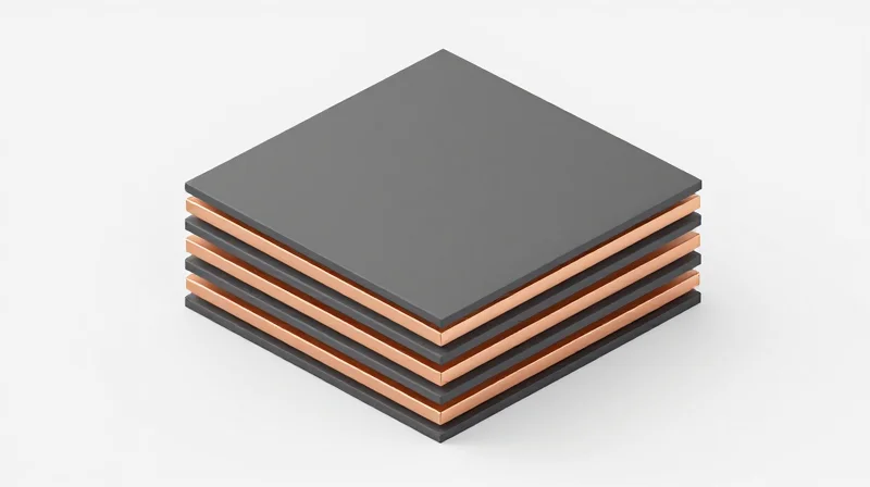
Achieving Symmetry for Signal Integrity and Mechanical Stability
A symmetric stack-up is the cornerstone of high-frequency design, serving dual purposes: maintaining consistent impedance profiles across all layers and preventing board warpage during the thermal cycling inherent in reflow soldering. By balancing the copper distribution and dielectric thicknesses around the board's physical center, you ensure that stresses are equalized, effectively mitigating the risk of delamination and registration shifts that can catastrophically degrade signal performance.
Strategic Use of Reference Planes
Impedance control relies heavily on a stable reference path. Every high-speed signal must have a continuous, low-impedance return path, typically provided by a solid ground or power plane. Discontinuities in these planes—caused by voids, splits, or crossing over board edges—create localized impedance spikes and increased electromagnetic interference (EMI).
| Feature | Best Practice | Risk if Ignored |
|---|---|---|
| Copper Balancing | Distribute copper evenly on all layers | Thermal warping and bowing |
| Reference Planes | Ensure solid, contiguous return paths | Reflections and EMI radiation |
| Dielectric Layout | Maintain symmetry across stack center | Differential skew and impedance mismatch |
Frequently Asked Questions
- How does stack-up asymmetry contribute to board warpage?
Asymmetry leads to unequal thermal expansion coefficients across the board structure. During high-temperature reflow processes, these unbalanced forces induce mechanical stress, resulting in bowing or twisting that can break via connections. - Can I use split planes to save space in high-frequency designs?
It is generally discouraged. Split planes disrupt the return current path, forcing signals to take circuitous routes, which introduces significant crosstalk and impedance discontinuities. - What is the primary role of prepreg in a symmetric stack-up?
Prepreg acts as the bonding agent. Using consistent prepreg types and thicknesses in symmetric layers is vital to achieving identical dielectric heights and consistent impedance for both top and bottom signal layers.
Trace Geometry: Width, Spacing, and Copper Weight
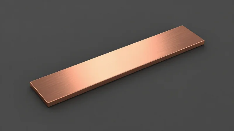
The Impact of Copper Geometry on Impedance
Impedance is fundamentally governed by the ratio of the signal trace width to the dielectric height, relative to the reference plane. Because etching is a subtractive process, chemical variables during manufacturing create a trapezoidal trace cross-section rather than a perfectly rectangular one. This "etch factor" results in a narrower base than the top, significantly shifting the intended impedance target if not accounted for during the design phase.
Managing Trace Width and Copper Weight
Copper weight directly influences the effective thickness of the conductor and the severity of undercut during etching. Heavier copper foils (e.g., 2 oz or greater) are more susceptible to significant undercut because the etchant must act for a longer duration, leading to wider top-to-bottom variations. For tight impedance tolerances, designers should prioritize the use of thinner copper (0.5 oz or 1 oz) to maintain higher geometric fidelity.
| Copper Weight | Etch Factor Sensitivity | Impedance Stability |
|---|---|---|
| 0.5 oz | Low | Excellent |
| 1.0 oz | Moderate | Good |
| 2.0 oz+ | High | Requires Compensation |
Guidelines for Trace Spacing and Tolerancing
Maintaining consistent trace spacing is vital for differential pair integrity. Variations in spacing directly impact odd-mode impedance. Designers must verify that their minimum trace-to-trace spacing accounts for both fabrication limits and the dielectric constraints of the chosen substrate.
- How does copper plating thickness affect my impedance?
Increased plating thickness increases the trace cross-sectional area, which lowers impedance. Designers must include the final plated thickness, not just the base foil weight, in their impedance simulations. - What is an acceptable impedance tolerance?
Standard industry tolerance is +/- 10%. For high-performance, high-speed signals, targeting +/- 5% is recommended, though this requires stricter material control and close collaboration with the PCB fabricator. - Should I add trace width compensation to my Gerber files?
No. Modern fabricators calculate the necessary etch compensation based on their specific process chemistry and material stack. Over-compensating in your design files will likely lead to incorrect trace geometries.
The Impact of Solder Mask on Impedance Calculations
Designers often overlook the solder mask during initial impedance modeling, yet it can introduce a measurable shift—typically between 2 to 5 ohms—in single-ended and differential impedance results. Because the solder mask has a different dielectric constant (Dk) than the underlying PCB core or prepreg, its application over traces effectively acts as a capacitive load, potentially slowing signal velocity and shifting the characteristic impedance lower.
Mechanisms of Impedance Shift
The impact of solder mask is most pronounced on microstrip configurations where traces are directly exposed to the outer environment. The mask covers both the copper trace and the adjacent laminate, creating a composite dielectric interface. The primary variables influencing this shift include the mask thickness (usually 0.5 to 1.5 mils) and the Dk, which typically ranges from 3.0 to 4.0 depending on the chemistry.
| Parameter | Effect on Impedance | Engineering Consideration |
|---|---|---|
| Increased Mask Dk | Decrease | Higher capacitance lowers characteristic impedance. |
| Increased Mask Thickness | Decrease | Greater volume of low-speed dielectric surrounds trace. |
| Complete Coverage | Stable | Consistency is key to preventing impedance variations. |
DFM Best Practices for Mask Sensitivity
- Should I include solder mask in my impedance models?
Yes. If your impedance tolerance is tight (e.g., +/- 5%), you must request your fabricator to account for the specific mask Dk and typical applied thickness in their field solver calculations. - How does solder mask dam affect impedance?
Variation in solder mask application—such as uneven coverage or 'dams' between pads—creates non-uniform impedance along the length of a trace, leading to signal reflections and potential EMI issues. - What is the best way to mitigate these shifts?
Work with your fabricator to define a 'mask-defined' or 'non-mask-defined' strategy. For critical high-speed traces, some designs explicitly specify 'mask-free' zones over long trace runs to ensure maximum impedance stability.
Ultimately, failing to communicate your impedance requirements relative to the solder mask application will result in 'golden board' discrepancies. Always ensure your design documentation explicitly states whether your impedance targets assume the presence of solder mask and at what thickness.
Communicating Effectively with Your PCB Fabricator
When designing for controlled impedance, the gap between engineering intent and manufacturing reality is bridged solely by the clarity and completeness of your documentation. Relying on default settings or ambiguous notes often leads to catastrophic impedance mismatches; therefore, providing a detailed fabrication drawing and explicit impedance specifications is non-negotiable.
Essential Fabrication Documentation
A robust fabrication package must explicitly define the stack-up geometry and the expected impedance targets for each layer. Do not leave the stack-up design to the fabricator's discretion without verification; instead, include a 'controlled impedance stack-up drawing' that clearly identifies material types, dielectric thicknesses, and the required copper weights for every layer.
| Documentation Element | Purpose | Risk if Omitted |
|---|---|---|
| Stack-up Drawing | Defines layer sequence and thickness | Unexpected impedance due to material changes |
| Impedance Table | Lists target ohms and tolerances | Uncontrolled signal reflections |
| Coupon Placement | Defines test structure locations | Inability to verify board performance |
Defining Impedance Coupons and Testing
Impedance coupons are the benchmark by which the fabricator proves your board meets the design specifications. Without these coupons, you are flying blind regarding the actual dielectric properties and etching accuracy achieved during the production process.
- How should I specify coupons?
Explicitly define the coupon type (e.g., TDR or VNA), location on the panel, and the specific traces they must represent. Request that these be etched alongside your production panel. - What tolerance should I dictate?
Standard industry tolerance is +/- 10%. If your signal integrity requirements demand tighter control, such as +/- 5%, ensure this is noted prominently on the fabrication drawing to avoid automatic rejection. - Why is the dielectric constant (Dk) important here?
Fabricators use different resins and glass weaves. Always provide the target frequency for your impedance measurements so the fabricator can use the appropriate Dk value for their calculations.
Proactive Communication Checklist
1. Provide a stack-up drawing including all dielectric constants.
2. List explicit impedance target values with specific tolerances.
3. Request a pre-production stack-up review for impedance verification.
4. Define trace/space width and copper weight constraints.
5. Confirm coupon locations on the manufacturing panel.
Best Practices for Impedance Testing and Coupons
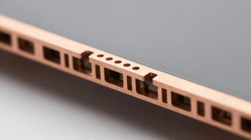
Impedance test coupons are essential diagnostic tools that bridge the gap between theoretical CAD models and physical board performance. By placing these dedicated structures on the panel perimeter, engineers can verify the dielectric constant and trace etching precision without destroying the actual functional circuitry of the PCB.
Strategic Design and Placement
A test coupon must be an exact representation of the production signal layers. It should include the same trace width, spacing, and reference plane configuration as the target design. Ideally, coupons should be placed in the panel rails or at the corners of the fabrication panel to capture process variations across the entire surface area.
| Feature | Best Practice | Impact |
|---|---|---|
| Location | Panel Rails/Edges | Captures etching variances |
| Geometry | Mirror Production | Ensures measurement accuracy |
| Connectivity | Ground/Signal Vias | Enables probe access |
Common Implementation FAQs
- Why should I include coupons if my board is high-volume?
Coupons provide a non-destructive verification method; without them, you would have to destructively cross-section boards to measure trace geometry, which is costly and time-prohibitive. - Does the solder mask on the coupon matter?
Yes. If the final production board will have solder mask, the coupon must also include it, as the dielectric constant of the mask significantly lowers the impedance of microstrip traces. - What is the industry standard for coupon length?
The trace length on a coupon must be sufficient to allow for a stable reading during Time Domain Reflectometry (TDR) testing, typically requiring a length of at least 3 to 6 inches depending on the signal rise time.
Verification Workflow
To master the verification process, align your requirements with the IPC-2141 standard. Always perform TDR testing immediately following etching and plating. If your impedance readings deviate by more than 5-10% from the target, investigate the copper etch factor and the actual thickness of the prepreg layers, as these are the primary culprits in impedance drift.
Common DFM Pitfalls and How to Avoid Them
Design for Manufacturing (DFM) oversights in high-speed, impedance-controlled designs often result in signal integrity degradation and costly fabrication re-spins. By identifying common pitfalls early in the design cycle, engineers can ensure that the physical implementation aligns with electromagnetic simulations.
Common DFM Pitfalls
- Reference Plane Discontinuities
Routing traces across split planes or voids in the reference layer causes severe impedance spikes and EMI issues. Always ensure a continuous return path under every signal line. - Inconsistent Dielectric Thickness
Failing to account for resin content variations or prepreg shrinkage leads to unexpected impedance shifts. Coordinate with the fabricator to specify controlled-impedance stack-up requirements. - Overlooking Solder Mask Effects
Ignoring the dielectric constant and thickness of the solder mask can lead to a 2-5 Ohm error. Always include solder mask in field solver calculations if precise tolerances are required. - Non-Standard Via Configurations
Uncontrolled via stub lengths or poor transition geometry create parasitic capacitance. Use back-drilling or optimized transition designs to maintain signal integrity.
Mitigation Strategy Comparison
| Pitfall | Impact | Avoidance Strategy |
|---|---|---|
| Plane Gaps | High Reflection/EMI | Bridge gaps with stitching caps or reroute signals. |
| Dielectric Variance | Impedance Mismatch | Use stack-up 'balanced' construction and consult material datasheets. |
| Via Stubs | Signal Resonance | Implement back-drilling for high-speed differential pairs. |
Engineering Best Practices
To effectively minimize these risks, integrate a DFM review process into your workflow. Utilize automation scripts to check for reference plane continuity, and always conduct a post-layout analysis that includes manufacturing tolerances. Engaging the PCB fabricator's engineering team during the stack-up definition phase is the single most effective way to eliminate ambiguities regarding dielectric properties and etching factors.
Successfully mastering impedance-controlled DFM is the difference between a prototype that works in the lab and a production run that fails in the field. By aligning your design constraints with the physical capabilities of your manufacturing partner, you can ensure high signal integrity at every turn. Ready to optimize your high-speed designs? Contact our engineering team today to review your next complex PCB project.
