
In the world of industrial automation, the difference between a reliable PLC and a system-wide failure often comes down to the integrity of the PCB design. As industrial environments grow increasingly electrically noisy, engineers must move beyond basic manufacturing constraints to implement advanced DFM rules. This article outlines the essential strategies for grounding, shielding, and layer configuration required to achieve rigorous EMI compliance and ensure long-term operational stability.
Understanding the High-Noise Industrial Environment
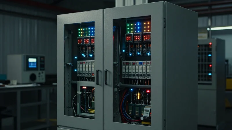
The Industrial Electromagnetic Landscape
Industrial environments are inherently hostile to precision electronics. Programmable Logic Controllers (PLCs) must operate reliably while surrounded by significant sources of Electromagnetic Interference (EMI) and transient voltage spikes. Unlike controlled data centers, industrial floors house heavy machinery that generates high-frequency noise, magnetic fields, and inductive kickback, all of which threaten the integrity of low-voltage logic circuits.
Primary Noise Sources in PLC Environments
| Source | Interference Type | Propagation Mechanism |
|---|---|---|
| Variable Frequency Drives | PWM Switching Noise | Radiated and Conducted |
| Inductive Loads (Contactors) | Back-EMF Transients | Conducted/Crosstalk |
| Large Motors | High Magnetic Flux | Radiated/Inductive Coupling |
| Welding Equipment | Wideband EMI | Radiated |
Analyzing Interference Mechanisms
Understanding the interaction between noise sources and PCB traces is essential for effective DFM. Interference typically manifests through three paths: capacitive coupling (dE/dt), inductive coupling (dI/dt), and direct conducted entry through power and I/O lines. A PLC PCB failing to account for these mechanisms will experience jitter, bit errors, or permanent hardware latch-up.
- How does VFD switching impact PCB signal integrity?
The high-speed switching of IGBTs in VFDs generates steep voltage edges (dv/dt) that couple into nearby signal traces, leading to common-mode noise that can override logic transitions. - Why are inductive transients particularly dangerous for PLCs?
When inductive loads like relays or motors are switched off, the collapse of the magnetic field causes a high-voltage flyback transient. If not properly clamped, this spike can exceed the breakdown voltage of semiconductor devices. - What is the most effective defense against radiated EMI on a PCB?
Adopting a solid reference plane, optimizing trace geometry to minimize loop area, and ensuring high-frequency decoupling are the primary DFM strategies to minimize susceptibility to external fields.
Advanced Grounding Strategies for PLC Boards
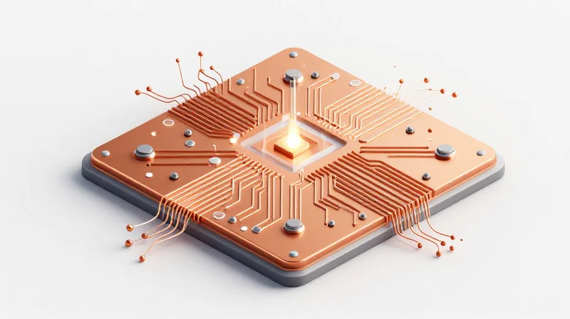
In industrial PLC design, grounding is not merely about safety; it is the foundational strategy for noise immunity. To mitigate the high-frequency transients typical of motor controllers and inductive switching, designers must transition from simple chassis connections to high-frequency, low-impedance grounding architectures.
Grounding Topologies: Single-Point vs. Multi-Point
| Strategy | Best Use Case | EMC Limitation |
|---|---|---|
| Single-Point (Star) | Low-frequency/DC signals | High-frequency common impedance coupling |
| Multi-Point | High-frequency/RF signals | Risk of ground loops |
| Hybrid Grounding | Mixed-signal PLC backplanes | Requires strict path control |
For modern PLC boards, multi-point grounding is mandatory for high-speed digital switching, as it provides a lower impedance path for return currents at frequencies above 1 MHz. However, this must be paired with low-inductance connection points to the chassis to prevent radiated emissions.
Optimizing the Ground Return Path
Return current always follows the path of least impedance. At high frequencies, this path is directly beneath the signal trace to minimize the loop area. Disrupting this path with slots or splits in the reference plane forces the current to take a longer path, resulting in increased loop area and significant radiated EMI.
- How do I handle return paths with split planes?
Avoid crossing gaps with high-speed signals. If a signal must cross a split, provide a stitching capacitor near the signal trace to provide a high-frequency bridge for return current. - Why is chassis grounding crucial for PLC boards?
A high-quality chassis connection acts as a low-impedance sink for common-mode currents, preventing noise from being injected into the internal signal ground reference. - What is the impact of ground vias?
Vias add series inductance. Use multiple stitching vias for ground plane transitions to reduce total path inductance, especially for high-speed digital I/O traces.
Optimized PCB Layer Stack-up Configurations
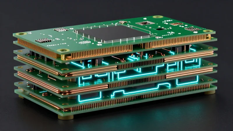
The Four-Layer Standard for Industrial Reliability
For industrial PLC applications, a four-layer stack-up is the minimum requirement to ensure reliable signal integrity. By dedicating internal layers exclusively to solid ground and power planes, designers create a low-impedance return path that is critical for mitigating noise coupling from external transients. This configuration minimizes loop area, which is the primary driver of radiated EMI.
Comparative Analysis of Stack-up Configurations
| Stack-up Type | EMI Performance | Signal Integrity | Cost/Complexity |
|---|---|---|---|
| 2-Layer (Signal/Signal) | Very Poor | Poor | Low |
| 4-Layer (Sig/GND/PWR/Sig) | Good | Moderate | Medium |
| 6-Layer (Sig/GND/Sig/Sig/PWR/Sig) | Excellent | High | High |
Essential Rules for Reference Plane Integrity
- Maintain Continuous Reference
Never route high-speed signals over splits in the reference plane. A gap in the plane forces return currents to take a longer path, creating a dipole antenna effect that generates significant EMI. - Stitching Vias
Place stitching vias at intervals along the edges of the board and near signal layer transitions to connect ground planes, effectively suppressing edge radiation. - Stack-up Symmetry
Always design the stack-up to be symmetrical around the center axis of the board to prevent physical warping during the reflow soldering process.
Addressing Split Planes in PLC Designs
In PLC modules where sensitive analog measurement circuits coexist with high-speed digital processing, split planes are often necessary to isolate noisy switching current. However, they must be implemented with caution. When splitting planes, use a bridge at the location of the signal trace transition to provide a defined return path. Failure to bridge a split results in significant common-mode noise, compromising the accuracy of industrial sensor inputs.
Mitigating Parasitic Capacitance and Inductance
Controlling Parasitic Effects in PLC Design
Parasitic capacitance and inductance act as unintended circuit elements that degrade signal performance, manifest as crosstalk, and contribute to EMI emissions. In industrial PLC environments, these effects are exacerbated by high-speed digital switching and rapid voltage transients. By minimizing loop areas and controlling trace coupling, designers can significantly reduce the coupling of high-frequency noise into sensitive control paths.
Strategies for Inductance Reduction
Loop inductance is proportional to the area enclosed by the signal and its return path. To minimize this, designers should adhere to strict return-path management practices. Keeping return paths directly beneath high-speed signals reduces the loop area and minimizes the flux linkage that causes electromagnetic interference.
| Design Factor | Effect on Parasitics | Mitigation Strategy |
|---|---|---|
| Trace Width | Increases Capacitance | Use minimum required width for current |
| Trace Length | Increases Inductance | Keep traces as short as possible |
| Via Placement | Adds Discontinuities | Use stitching vias for plane transitions |
| Board Spacing | Coupling susceptibility | Maintain 3H rule for isolation |
Mitigating Parasitic Capacitance
Parasitic capacitance occurs primarily between adjacent traces or planes. Excessive capacitance between high-speed signals and ground planes can lead to signal ringing or excessive driver loading. To mitigate this, avoid long parallel runs between sensitive analog signals and high-speed digital switching lines.
- How can I reduce trace-to-trace crosstalk?
Increase the space between parallel traces to at least three times the trace width (the 3W rule) or introduce a grounded guard trace to redirect capacitive coupling. - Why is minimizing via count important?
Every via adds parasitic capacitance and inductance, acting as a small discontinuity that can cause signal reflection and impedance mismatch. - What role does substrate thickness play?
Thinner dielectrics between a signal layer and its reference plane reduce loop inductance by minimizing the vertical separation between the signal and return path.
Trace Routing and Signal Integrity in Digital and Analog Sections
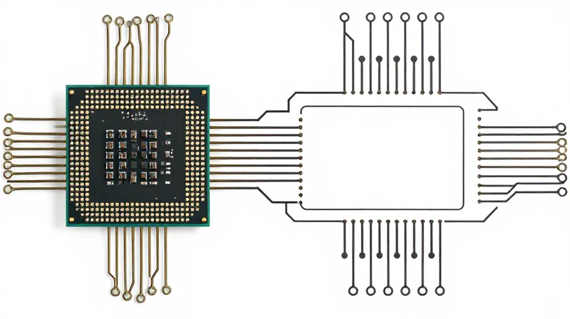
Partitioning and Trace Routing Strategies
The fundamental design strategy for a robust PLC PCB is the strict segregation of signal domains. By physically isolating the 'noisy' digital section—typically containing microcontrollers, communication interfaces, and high-speed switching transistors—from the 'quiet' analog section, which handles low-voltage sensor inputs, engineers can prevent digital switching noise from contaminating precision signals.
- How does trace routing affect crosstalk?
Parallel high-speed digital traces act as antennas, inducing inductive coupling in nearby sensitive analog lines. Route sensitive lines on different layers and maintain a minimum clearance of at least 3x the dielectric height from any digital switching signal. - What is the role of the return path?
Signal integrity relies entirely on the return path. Every digital signal must have a continuous reference plane beneath it. Interrupting this plane forces the return current to take a longer path, increasing loop area and radiated emissions.
Signal Integrity Comparison
| Design Factor | Analog Section | Digital Section |
|---|---|---|
| Trace Width | Thicker for low impedance | Determined by characteristic Z |
| Grounding | Star ground/Dedicated plane | Multi-point/Common plane |
| Component Placement | High density near A/D converter | Separated by isolation moats |
Mitigating High-Frequency Coupling
To further protect analog inputs from digital transient spikes, implement a 'moat' (a deliberate gap in the power and ground planes) if the application demands extreme isolation. However, ensure that any signal trace crossing this moat is bridged by a decoupling capacitor or a specialized isolator (e.g., digital isolators or optocouplers) to avoid creating a massive return-current loop. Utilizing differential pair routing for analog inputs further enhances common-mode rejection, ensuring that industrial noise coupled onto the lines is canceled out at the receiver input.
Component Selection for Enhanced EMI Robustness
Component Selection for Enhanced EMI Robustness
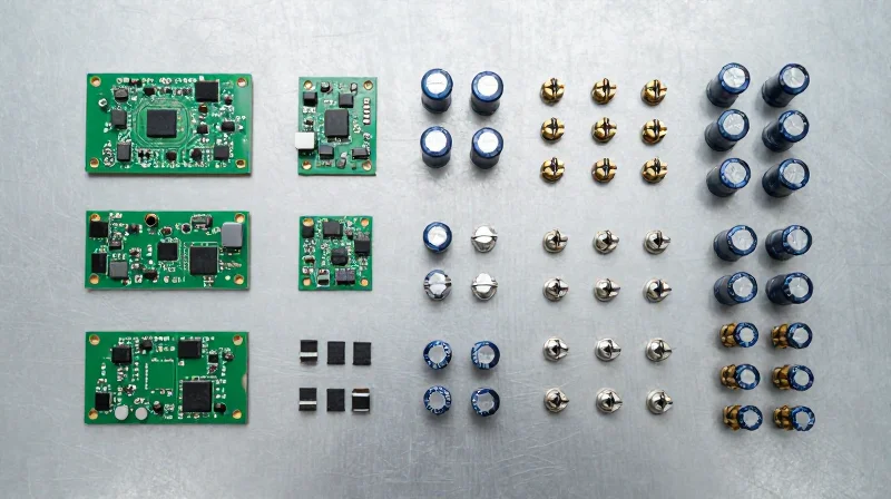
Achieving industrial-grade EMI performance requires moving beyond standard component selection to focus on electromagnetic compatibility (EMC) characteristics and physical placement strategies. By prioritizing low-ESR capacitors, ferrite beads with optimized impedance profiles, and high-energy transient suppressors, designers can effectively suppress common-mode noise and protect sensitive logic from harsh electrical environments.
Critical Component Strategies
| Component Type | EMI Function | Design Rule |
|---|---|---|
| Decoupling Caps | Local Energy Reservoir | Place X7R/C0G ceramics as close as possible to IC VCC pins. |
| Ferrite Beads | High-Frequency Filtering | Place in series with power rails; match current rating to load. |
| TVS Diodes | Transient Protection | Route traces through the diode before the protected IC pin. |
Frequently Asked Questions on Component DFM
- Why is the placement of decoupling capacitors critical?
Long traces between a capacitor and a power pin introduce parasitic inductance, which effectively disconnects the capacitor at high frequencies and allows noise to propagate. - What is the best way to route TVS diodes for ESD protection?
The signal must pass through the TVS diode connection point before reaching the target IC to ensure the clamping current does not spike the voltage at the protected input. - How do I choose the right ferrite bead for EMI suppression?
Select a bead where the impedance peak aligns with the frequency range of the observed noise, while ensuring the DC resistance is low enough to prevent significant voltage drop.
DFM Compliance Testing and Verification
Bridging Simulation and Compliance
Design for Manufacturing (DFM) and EMC compliance are not static goals but are iterative outcomes of pre-production validation. While software simulations provide a baseline, compliance requires verifying these models against physical reality. For industrial PLCs, meeting IEC 61131-2 requires validation of signal integrity, immunity to electromagnetic disturbances, and thermal reliability under high-load conditions.
| Verification Method | Primary Goal | Industrial Standard Focus |
|---|---|---|
| Full-Wave EM Simulation | Identify resonance & radiation | IEC 61000-4-3 (Radiated Immunity) |
| TDR Analysis | Verify impedance continuity | Signal Integrity (High-speed bus) |
| Thermal Imaging | Validate power density | IEC 61131-2 (Thermal Stability) |
| ESD Gun Testing | Verify surge protection | IEC 61000-4-2 (ESD Immunity) |
Interpreting Simulation Data for DFM
Simulation data must be interpreted through the lens of manufacturing tolerances. A trace that shows perfect impedance in a CAD model may fail in production due to dielectric constant (Dk) variation in FR-4 substrates. Engineers should apply a 10% safety margin in simulation to account for manufacturing variances.
- How do I ensure simulation accuracy?
Utilize verified component models from manufacturers and include parasitic values for all decoupling capacitors and vias in your simulation netlist. - What should I look for in frequency sweep reports?
Monitor for unexpected resonant peaks in the 30 MHz to 1 GHz range, as these are primary indicators of potential EMI failure in industrial environments. - Why do physical prototypes still fail EMC tests despite clean simulations?
Physical failures often stem from incorrect grounding strategies, such as floating planes or inadequate stitching via density, which simulation models may omit if the layout environment is oversimplified.
Standardized Pre-Compliance Workflow
1. Layout Rule Check (DRC/ERC): Verify via stitching & spacing. 2. Signal Integrity Audit: Perform TDR simulations for high-speed differential pairs. 3. EM Field Mapping: Identify hot spots at 100MHz+ harmonics. 4. Margin Adjustment: Apply 10% tolerance to all impedance targets. 5. Thermal Stress Test: Simulate heat dissipation at worst-case PLC load.Future-Proofing Your PLC Designs
Designing for Extended Lifecycles
To ensure long-term reliability in industrial environments, designers must prioritize component longevity, modularity, and thermal management. Future-proofing is not merely about over-engineering but selecting components with high mean time between failures (MTBF) ratings and verified supply chain stability. By adopting a 'Design for Repair and Upgrade' philosophy, engineers can maintain performance standards even as legacy components phase out.
Cost vs. Durability Matrix
| Design Strategy | Initial Cost Impact | Long-term Value | Risk Mitigation |
|---|---|---|---|
| Standard Grade Components | Low | Low | High failure rate under thermal stress |
| Industrial/Automotive Grade | Moderate | High | Proven resilience in harsh environments |
| Hardware Modularity | Moderate | Very High | Facilitates rapid field repairs and upgrades |
Strategic DFM Considerations for Longevity
- How does PCB material selection impact 10-year durability?
Utilizing high-Tg (glass transition temperature) FR-4 materials prevents delamination and impedance instability caused by constant thermal cycling in industrial cabinets. - Why should I avoid 'bleeding-edge' components?
New silicon often lacks the long-term field data needed for industrial certification; choosing mature, widely supported architectures ensures easier sourcing and firmware stability over a decade. - What role does conformal coating play in future-proofing?
Applying industrial-grade conformal coatings at the DFM stage protects against humidity, chemical fumes, and conductive dust, effectively extending the physical life of the PCB assembly.
Maintenance and Verification
Future-proof designs must incorporate accessible test points and diagnostic LEDs to streamline field maintenance. When verifying designs against standards like IEC 61131-2, prioritize modular firmware updates and programmable gate arrays (FPGAs) to allow for minor logic adjustments without requiring costly hardware board spins.
Successfully designing for industrial applications requires a deep commitment to electromagnetic compatibility and signal integrity. By applying these advanced DFM strategies, you can reduce production failures and field service calls significantly. If you are ready to elevate your board design process, contact our engineering team today for a comprehensive design audit or to consult on your next high-performance PLC project.
