
The factory floor is undergoing a seismic shift. As we move deeper into the era of Industry 4.0, the traditional Programmable Logic Controller (PLC) is being pushed beyond its original design boundaries to meet the demands of real-time data integration and high-speed communication. This article examines how modern PLC hardware architectures are evolving and why mastering complex EMC challenges is now the ultimate differentiator for industrial manufacturers.
The Evolution from Legacy to Industry 4.0 PLC Architectures
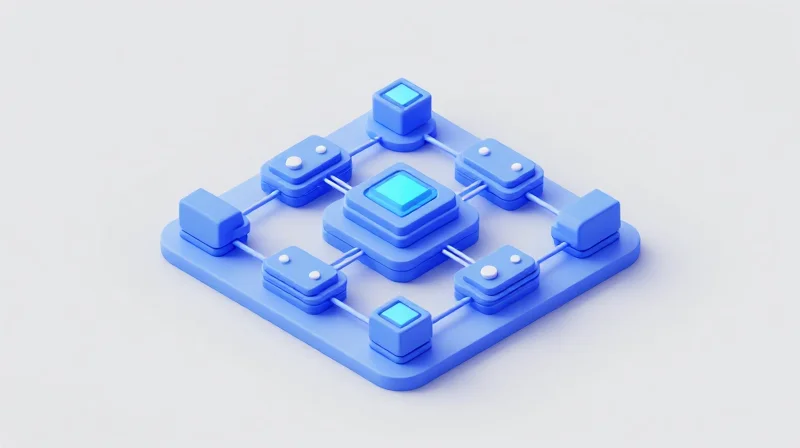
From Monolithic Foundations to Distributed Intelligence
Legacy PLC architectures were defined by centralized, rack-based hardware where a single powerful processor handled all I/O logic and execution within a physically confined environment. While robust for simple automation, this design inherently bottlenecks high-speed data acquisition and real-time analytical processing. The shift toward Industry 4.0 demands a paradigm shift: moving from monolithic processors toward distributed, modular PCB designs where intelligent edge nodes perform local data processing, reducing latency and reliance on a central backplane.
| Feature | Legacy Architecture | Industry 4.0 Architecture |
|---|---|---|
| Processing Topology | Centralized | Distributed |
| Scalability | Hardware dependent | Software-defined/Modular |
| Data Handling | Cyclic scanning | Event-driven/Asynchronous |
| Connectivity | Fieldbus-centric | OPC UA/TSN-enabled |
Architectural Shifts in PLC PCB Design
Modern PLC PCB design focuses on thermal efficiency and signal integrity at higher clock frequencies. To accommodate the increase in communication density, next-gen boards utilize multi-layer PCB stack-ups with high-density interconnect (HDI) technology. This allows for complex system-on-module (SoM) integration, effectively isolating power-hungry high-speed processing from sensitive analog I/O circuitry to improve signal-to-noise ratios and electromagnetic compatibility.
- What defines the shift in PCB power management?
Industry 4.0 architectures move toward distributed point-of-load regulation, minimizing the EMI footprint associated with long-trace power distribution found in legacy rack systems. - Why are modular architectures prioritized?
Modular designs allow for independent hardware upgrades and firmware maintenance, significantly reducing downtime and enabling predictive maintenance capabilities at the source.
High-Speed Signal Processing: The New Hardware Standard

The Shift to High-Bandwidth Processing Architectures
Modern industrial control systems have outgrown the limitations of traditional microcontroller-based architectures. To support the high-frequency deterministic requirements of Industry 4.0, PLC manufacturers are transitioning to heterogeneous computing architectures. By offloading time-critical communication and signal processing tasks to FPGAs or high-performance System-on-Chip (SoC) devices, these systems can achieve sub-microsecond latency, essential for high-speed motion control and real-time machine vision.
| Architecture | Signal Processing Capability | Best Use Case |
|---|---|---|
| Legacy MCU | Low/Moderate (Sequential) | Slow I/O, Basic Sequencing |
| FPGA-Based | Extreme (Parallel Logic) | High-Speed Motion, Precise Timing |
| SoC (CPU + FPGA) | Superior (Hybrid Processing) | Advanced Analytics, Real-Time Fieldbus |
Challenges in High-Speed Signal Integration
- How does signal integrity impact board layout?
As clock frequencies rise to support faster processing, PCB traces must be treated as transmission lines to minimize crosstalk and electromagnetic interference, often requiring multi-layer boards with dedicated ground planes. - What is the primary role of FPGAs in industrial communication?
FPGAs handle the deterministic hardware-level protocol stacks (like EtherCAT or PROFINET IRT) that CPUs cannot process reliably, ensuring predictable packet delivery regardless of system load. - Do higher clock speeds worsen EMC compliance?
Yes, higher-frequency components increase the risk of radiated emissions; therefore, modern PLC designs must incorporate advanced signal shielding and controlled-impedance routing to comply with stringent EMC regulations.
The integration of these high-speed architectures necessitates a paradigm shift in PCB design. Engineers must balance the computational power of the SoC with the physical constraints of thermal management and signal noise immunity, ensuring that the hardware remains robust enough for harsh industrial environments while delivering unprecedented data throughput.
PCB Design Strategies for Increased Component Density
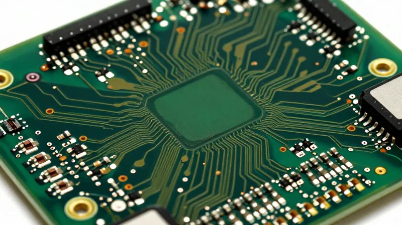
Advanced Fabrication and Layout Techniques
As PLC modules shrink to fit into high-density industrial enclosures, designers must transition from traditional 4-6 layer boards to High-Density Interconnect (HDI) structures. Utilizing micro-vias, via-in-pad technology, and buried/blind vias allows for increased routing density without compromising board reliability. By minimizing trace length between high-speed SoC components and their associated power delivery networks, designers can effectively reduce parasitic inductance—a critical factor in maintaining signal integrity in dense environments.
Thermal and Signal Integrity Trade-offs
| Strategy | Density Benefit | Integrity/Thermal Impact |
|---|---|---|
| HDI Micro-vias | High | Improves signal routing; requires careful impedance matching. |
| Copper Coins | Medium | Superior thermal dissipation for high-power SoC chips. |
| Buried Capacitance | High | Reduces board footprint; enhances EMC filtering. |
Managing EMC in Compact Architectures
- How does component density impact EMC?
Increased density brings sensitive high-speed signals closer to switching power supplies, heightening the risk of crosstalk and electromagnetic interference (EMI). - What is the best approach for grounding in dense PLCs?
Implement a solid, continuous ground plane layer directly adjacent to high-speed signal layers to ensure a low-impedance return path and reduce loop areas. - How can thermal integrity be maintained in small footprints?
Utilize thermal vias and localized metal heat spreaders, or transition to high-thermal conductivity substrate materials like metal-core PCBs where applicable.
Navigating the New Landscape of EMC Challenges
The EMC Paradox: Speed versus Stability
Modern PLC architectures rely on rapid signal switching to support real-time Industrial Ethernet protocols like TSN (Time-Sensitive Networking). However, this increase in edge rates results in higher harmonic content, directly increasing radiated emissions. As component density on the PCB grows, traditional passive filtering techniques often fail, as parasitic capacitance and mutual inductance between traces become dominant sources of crosstalk and electromagnetic interference.
Comparative Impact of Design Transitions
| Design Factor | Legacy Architecture | Next-Gen Architecture | EMC Impact |
|---|---|---|---|
| Switching Speed | kHz range | MHz+ (Edge rates) | Increased harmonic emission |
| Component Density | Low/Moderate | Ultra-High | Severe trace coupling |
| Grounding Strategy | Chassis focus | Multi-layer/Split planes | Complex return paths |
Critical EMC Mitigation Strategies
- How does signal integrity correlate with EMC?
Impedance discontinuities in high-speed transmission lines act as antennas, radiating energy. Maintaining strict 50-ohm or 100-ohm differential control is essential for preventing both reflection and EMI. - Can shielding overcome layout issues?
No; shielding is a secondary defense. Modern design must prioritize PCB-level stackup management—such as using dedicated ground planes directly under high-speed signals—to minimize return path loops at the source. - Why are emerging EMC standards more stringent?
As PLCs operate in closer proximity to sensitive IoT sensors and wireless modules, the noise floor tolerance has decreased, forcing designs to meet tighter limits on broadband electromagnetic noise.
Ultimately, the design of next-generation PLC hardware requires an iterative simulation approach. Electromagnetic Field (EMF) modeling must be integrated into the layout phase to identify hotspots before fabrication, as the high-frequency nature of these signals renders post-hoc shielding ineffective.
Advanced Shielding and Grounding Techniques

Advanced Shielding and Grounding Strategies
As PLC architectures transition toward higher-density SoC designs, traditional shielding methods often become inadequate. Modern strategies now shift toward active noise cancellation and localized electromagnetic containment to manage EMI without increasing device dimensions.
Comparison of Shielding Methodologies
| Method | Benefit | Footprint Impact |
|---|---|---|
| Board-Level Shielding (BLS) | High attenuation of localized RF | Requires clearance |
| Conductive Elastomer Gaskets | Flexible EMI sealing for complex geometry | Minimal |
| Differential Pair Via Fencing | Containment of high-speed transients | Negligible |
| Active Noise Cancellation | Adaptive mitigation of low-frequency noise | None (Circuit-based) |
Best Practices for Grounding in Dense Layouts
Grounding in high-density PLC boards requires a transition from traditional star-grounding to multi-layer stitched ground planes to ensure low-impedance paths for high-frequency return currents.
- How does stitching impact impedance?
Ground stitching vias effectively minimize the loop area of high-speed return paths, significantly reducing trace inductance and radiated EMI. - Is localized shielding better than enclosure shielding?
In high-frequency applications, localized board-level shielding is superior as it prevents crosstalk between high-speed logic and sensitive analog sensing circuits on the same substrate. - How do we maintain thermal integrity while shielding?
Using thermally conductive EMI gaskets or phase-change materials allows the shield to function as both an electromagnetic barrier and a primary heat-sink path.
The Role of Intelligent Power Management
In the context of modern industrial automation, the power delivery network (PDN) is no longer a passive utility but an active component in system integrity. As PLC architectures shift toward higher density and faster switching, intelligent power management must mitigate the transient noise induced by high-frequency power conversion, ensuring that sensitive analog input stages maintain high signal-to-noise ratios even amidst significant factory-floor electromagnetic interference.
Dynamic Noise Rejection and PDN Optimization
Modern PLC designs leverage advanced power ICs that feature programmable switching frequencies and spread-spectrum clocking. By dynamically adjusting the power stage behavior, designers can shift the fundamental switching noise outside the critical frequency bands of precision sensors. Furthermore, the integration of distributed point-of-load (PoL) regulation minimizes trace length, drastically reducing the antenna effect that facilitates EMI coupling onto sensitive signal lines.
| Feature | Legacy Approach | Next-Gen Intelligent Approach |
|---|---|---|
| Switching Frequency | Fixed frequency (static) | Adaptive / Spread-spectrum |
| Regulation Strategy | Centralized LDOs/Buck | Distributed digital PoL controllers |
| Noise Mitigation | Passive filter banks | Active EMI cancellation and active filtering |
Frequently Asked Questions
- How does digital power control improve EMC compliance?
Digital control allows for precise control of MOSFET gate drive rise times (slew rate control), which reduces high-frequency ringing and emissions at the source without requiring oversized passive components. - Why is isolation critical in high-density PLC power designs?
Robust galvanic isolation prevents ground loops and high-voltage transients from industrial machinery from propagating to low-voltage logic circuits, protecting sensitive sensor inputs from degradation. - Can intelligent power management reduce PCB footprint?
Yes, by increasing switching frequencies and using advanced integration, smaller magnetic components can be used, and the reduced need for bulky passive filtering allows for higher density layout.
Compliance and Reliability in a Connected World
Regulatory Compliance in High-Density PCB Design
As PLC architectures transition toward high-density interconnect (HDI) technologies to support edge computing, maintaining compliance with international standards such as IEC 61131-2 becomes increasingly complex. Reliability is no longer merely a function of robust casing but resides in the PCB stack-up and trace-routing strategy. Modern designers must reconcile miniaturization with the stringent clearance and creepage distances required to prevent electrical arcing and failures in harsh industrial environments.
Reliability Metrics and Testing Standards
| Standard | Focus Area | Impact on Architecture |
|---|---|---|
| IEC 61131-2 | PLC Hardware | Dictates isolation and environmental immunity |
| IEC 61000-4-x | EMC Immunity | Requires advanced filtering at board entry |
| ISO 13849-1 | Functional Safety | Mandates redundant design paths |
Frequently Asked Questions on Hardware Reliability
- How does thermal management impact long-term reliability?
Excessive heat leads to electromigration and accelerated aging of passive components. Next-gen architectures utilize localized thermal vias and copper planes to dissipate heat away from sensitive processing cores. - What role does conformal coating play in high-density PCBs?
Conformal coatings protect against conductive dust, moisture, and chemical vapors, which are common failure points in dense layouts where trace spacing is minimized. - Can software-defined features replace hardware reliability?
No; software can perform diagnostic monitoring, but inherent hardware reliability must be achieved through robust signal integrity and power management circuits first.
Expert Outlook: Preparing for the Next Decade of Automation
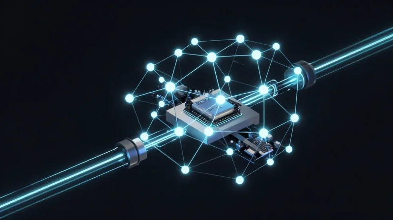
The Evolution of PLC Hardware Architecture
As we move toward the next decade, PLC hardware is shifting from monolithic blocks to modular, high-density architectures. Next-generation designs are prioritizing localized AI processing, enabling real-time edge analytics that reduce latency and minimize the need for heavy data transmission across noisy industrial networks.
| Feature | Legacy PLC Architecture | Next-Gen PLC Architecture |
|---|---|---|
| Processing | Centralized CPU | Distributed Edge AI |
| EMC Strategy | Passive Shielding | Active Noise Cancellation |
| Connectivity | Fieldbus-heavy | Ethernet/TSN-Native |
| Diagnostics | Post-failure analysis | Predictive/Proactive |
Material Science and Electromagnetic Resilience
The integration of wide-bandgap semiconductors like Gallium Nitride (GaN) is set to redefine efficiency in industrial power delivery. However, these components introduce high-frequency switching noise, necessitating a revolution in PCB material selection. We are observing a shift toward advanced dielectric substrates and integrated buried capacitance layers that naturally dampen parasitic oscillations at the board level.
Frequently Asked Questions on Future Industrial Trends
- How will AI change hardware maintenance?
AI will shift maintenance from reactive to predictive by monitoring electromagnetic signatures and heat maps on PCBs to detect component degradation before actual failure. - Is board miniaturization a threat to EMC compliance?
Miniaturization increases crosstalk, but it is being countered by high-density interconnect (HDI) technologies and advanced simulation-driven layout design that optimizes trace geometry for noise rejection. - What is the primary role of GaN in future PLCs?
GaN allows for smaller power stages with significantly higher efficiency, reducing thermal stress on critical components and enabling smaller form factors for modular, distributed control systems.
As industrial environments become more interconnected, the margin for error in PCB design and EMC compliance vanishes. Manufacturers must bridge the gap between traditional reliability and modern high-speed requirements to remain competitive. Contact our engineering consultancy team today to optimize your next-gen PLC architecture and stay ahead of the Industry 4.0 curve.
