
In the fast-paced world of industrial Human Machine Interfaces (HMI), even a minor deviation in PCB design can render a high-sensitivity touch panel unresponsive. As device footprints shrink and touch sensitivity demands rise, the gap between prototype success and mass-production failure often comes down to Design for Manufacturing (DFM). This guide provides the essential engineering framework to optimize your touch panel layouts for reliability and high performance.
The Anatomy of High-Sensitivity Touch Sensors
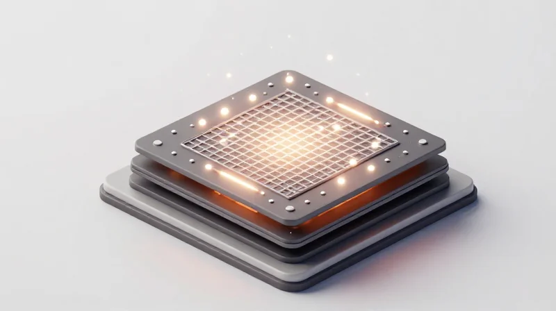
The performance of an industrial touch panel begins with the precise engineering of its sensor matrix. At its core, a high-sensitivity touch sensor operates by monitoring microscopic fluctuations in mutual or self-capacitance. In industrial settings, where electromagnetic interference (EMI) is prevalent, the anatomy of these sensors must be optimized not only for sensitivity but also for robust signal-to-noise ratio (SNR) management.
Capacitive Coupling Fundamentals
High-sensitivity sensors utilize a transparent conductive layer, typically Indium Tin Oxide (ITO) or metal mesh, etched into an X-Y grid pattern. When a conductive object like a human finger approaches, it creates a capacitive coupling effect that alters the electrical field between the transmit (TX) and receive (RX) nodes. In industrial design, the DFM process must account for the parasitic capacitance introduced by thick cover lenses and protective overlays, which can dampen the signal and raise the noise floor.
Technical Comparison: ITO vs. Metal Mesh
| Feature | ITO (Indium Tin Oxide) | Metal Mesh |
|---|---|---|
| Resistance | Higher | Extremely Low |
| Flexibility | Brittle | High |
| Suitability | Standard HMI | Large/High-Sensitivity |
| Visual Moire | Negligible | Potential issue |
Addressing the Noise Floor in Industrial Environments
- How does environmental EMI affect touch sensors?
Industrial machinery, high-voltage lines, and switching power supplies create ambient noise that can trigger false touches or 'ghosting' by overwhelming the sensor's baseline capacitance. - Why is trace routing critical for high sensitivity?
Improper trace routing increases parasitic capacitance and loop area, making the sensor more susceptible to external radiation, which effectively lowers the SNR. - What role does shielding play in DFM?
Integrated ground planes and active shielding layers are essential to isolate the sensing matrix from internal board noise, ensuring that only intentional touch inputs are processed.
Optimizing PCB Stack-up for EMI Shielding
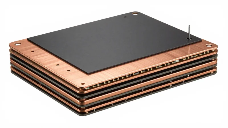
Strategic Stack-up Principles for Noise Mitigation
In industrial touch panel designs, the primary EMI challenge lies in the coupling between high-speed digital switching signals (such as display interfaces like MIPI or LVDS) and the ultra-sensitive capacitive touch sensing electrodes. Effective noise suppression requires a symmetric stack-up that mandates a dedicated ground plane adjacent to every signal layer.
| Stack-up Feature | Implementation Strategy | EMI Benefit |
|---|---|---|
| Layer Pairing | Always pair signal with an adjacent reference plane | Minimizes return path loops and radiated emissions |
| Prepreg Thickness | Minimize distance between signal and ground | Lowers inductance of return current paths |
| Ground Pouring | Avoid floating copper in touch areas | Prevents inadvertent antenna formation |
Isolating Analog and Digital Domains
To achieve maximum Signal-to-Noise Ratio (SNR) for touch inputs, the physical stack-up must logically separate domains. Place the touch-sensing traces on the outer layers to minimize capacitive coupling to internal digital logic, while ensuring that the internal routing for sensitive analog traces is shielded by solid ground pours on the layers immediately above and below.
Frequently Asked Questions
- Why should I avoid crossing gaps in the reference plane?
Crossing a gap forces return currents to take a longer path, creating a larger loop area that significantly increases EMI radiation and susceptibility to external noise. - Should I use power planes as return paths?
No. Always use a dedicated, solid ground plane to provide a low-impedance return path for high-frequency currents, ensuring stable reference potential for the touch controller. - How does PCB thickness affect touch performance?
Thinner stack-ups improve the coupling efficiency of the sensor electrode to the finger, but increase the risk of cross-talk if internal layer separation is not managed through robust ground shielding.
Critical Trace Routing and Impedance Control
Critical Trace Routing and Impedance Control
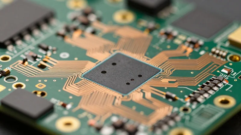
For touch panels, trace routing serves as the bridge between raw capacitive data and the sensing controller. Because touch signals are often extremely low-amplitude, impedance mismatch leads to reflections that manifest as jitter or phantom touches. Maintaining a controlled impedance, typically 50 ohms for signal lines or 90-100 ohms for differential pairs, is non-negotiable. Designers must ensure consistent trace widths and sufficient clearance from digital planes to prevent noise injection.
Routing Best Practices
- Length Matching
Keep trace lengths for parallel touch channels matched within 0.1mm to ensure signal arrival synchronization at the controller. - Via Usage
Minimize the use of vias in signal paths; every via transition introduces parasitic inductance that can degrade the noise floor. - Guard Traces
Implement ground guard traces between high-frequency digital lines and sensitive capacitive traces to provide a shielding barrier against crosstalk.
| Design Parameter | Recommended Industrial Standard | Impact on Performance |
|---|---|---|
| Trace Width Tolerance | +/- 10% | Reduces impedance fluctuations |
| Copper Weight | 0.5 oz (finished) | Balances trace etching and skin effect |
| Trace Separation | 3x Dielectric Height | Mitigates electromagnetic coupling |
Maintaining Impedance Stability
Industrial manufacturing processes can vary, impacting the final geometry of your traces. Always specify a 'Controlled Impedance' requirement in your fabrication notes and require the PCB vendor to perform TDR (Time Domain Reflectometry) testing. By providing a reference stack-up with specific dielectric constants (Dk), you enable the manufacturer to adjust trace width compensation (etch factors) to hit the target impedance accurately.
Mitigating Parasitic Capacitance in Design
Strategies for Minimizing Unwanted Coupling
Parasitic capacitance acts as a hidden enemy in touch sensor designs, coupling high-speed switching noise directly into sensitive analog nodes. To mitigate these effects, designers must prioritize maximizing physical distance between touch traces and noisy digital nets, utilizing dedicated ground planes as effective shields, and strictly controlling trace geometry to minimize surface area exposure.
Key Mitigation Techniques
| Technique | Implementation Priority | Impact on Parasitic Capacitance |
|---|---|---|
| Guard Tracing | High | Significantly reduces lateral coupling |
| Reduced Trace Length | Critical | Lowers total conductive surface area |
| Solid Ground Shielding | High | Prevents noise penetration from underlying layers |
| Via Elimination | Medium | Reduces vertical capacitive coupling |
Frequently Asked Questions
- How do guard traces reduce parasitic noise?
Guard traces are grounded traces placed parallel to sensitive signal traces. They create a low-impedance path to ground, shunting capacitive noise away from the touch electrode before it can interfere with the measurement signal. - Does solder mask thickness impact parasitic capacitance?
Yes, variations in solder mask thickness can change the dielectric constant environment around traces. Consistent application is crucial to ensure predictable capacitive coupling throughout the board life cycle. - Why is minimizing via count important for touch sensors?
Each via adds an localized increase in capacitance and potential for signal reflections. By keeping traces on a single layer, you eliminate these variables and maintain a stable, uniform dielectric interface for the sensor input.
Grounding Strategies for HMI Reliability
Implementation of Split-Ground Planes
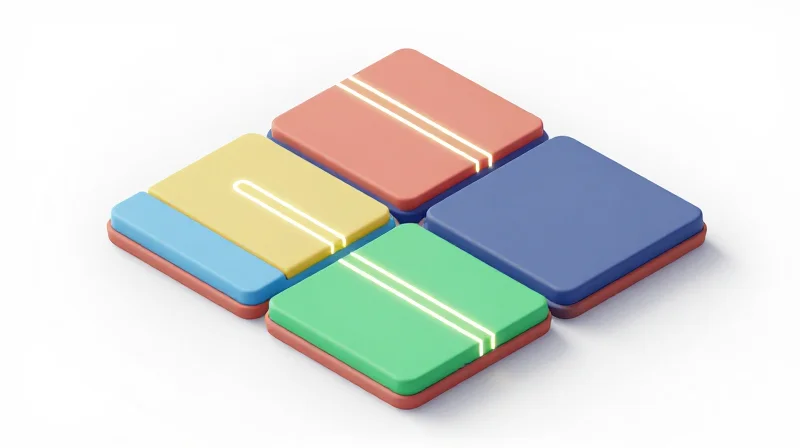
To achieve high reliability, it is critical to physically and electrically separate the noisy digital ground (DGND) from the sensitive analog touch-sensing ground (AGND). By employing split-ground planes, designers create dedicated return paths, preventing high-frequency digital return currents from injecting noise into the analog measurement front-end. The planes must only be connected at a single, well-defined point—typically at the analog-to-digital converter (ADC) or the main processor's reference point—to avoid creating ground loops.
Star Grounding vs. Plane Splitting
| Strategy | Primary Benefit | Best Application |
|---|---|---|
| Star Grounding | Eliminates loop currents by centralizing reference | Mixed-signal circuits with low complexity |
| Split Planes | Superior high-frequency isolation | High-speed HMI interfaces with digital noise |
Grounding Best Practices FAQ
- Can I route signals across a split in the ground plane?
No, routing high-speed signals across a split creates a slot antenna effect and interrupts the return current path, significantly increasing EMI emissions. - Where should the bridge between AGND and DGND occur?
The bridge must occur at the point where the signal crosses the boundary, ideally under the ADC to keep return loop areas minimized. - Does a continuous ground plane ever provide better performance?
In highly complex, high-speed designs, a single, solid reference plane is often superior to split planes, provided that components are strategically partitioned to prevent digital noise from entering sensitive areas.
DFM Rules for Solder Mask and Silkscreen
Solder Mask Design for High-Volume Assembly
In industrial touch panel manufacturing, solder mask registration is the primary defense against bridging, especially on fine-pitch components. Maintaining strict adherence to DFM standards ensures that solder dams remain intact during reflow.
| Feature | Standard Tolerance | Impact |
|---|---|---|
| Mask Expansion | 0.05mm - 0.075mm | Prevents copper oxidation and accidental solder bridging. |
| Solder Dam Width | Min 0.1mm | Ensures reliable isolation between fine-pitch pads. |
| Mask Registration | +/- 0.05mm | Critical for centering on BGA and QFN components. |
Silkscreen Best Practices for Industrial Clarity
While silkscreen does not affect electrical performance, its poor execution hampers automated visual inspection (AVI) and technician repair. Industrial standards require high-contrast, legible markings that avoid copper features to prevent adhesion failures.
- Why must silkscreen avoid pads?
Silkscreen ink on solder pads prevents proper wetting and creates uneven joints, which can lead to open circuits during the reflow process. - What is the recommended stroke width?
To ensure legibility under AVI systems, a minimum line width of 0.15mm to 0.20mm is recommended, maintaining a 0.25mm clearance from exposed copper.
Advanced Masking for Touch Interfaces
/* DFM Check List for Touch Panels */
check_solder_dam_min_width(0.1mm);
verify_silkscreen_to_pad_clearance(0.25mm);
validate_mask_expansion_uniformity();
Material Selection and Thermal Management
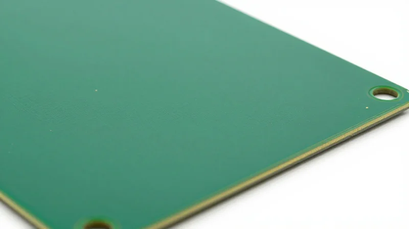
Substrate Selection for Industrial Reliability
Industrial touch panels require substrates that can withstand thermal cycling, moisture, and vibration. Standard FR-4 is often insufficient for extreme applications, necessitating higher glass transition temperature (Tg) materials to maintain structural integrity and prevent pad lifting during prolonged operation.
| Substrate Material | Key Benefit | Ideal Application |
|---|---|---|
| Standard FR-4 | Cost-effective | Indoor HMI, standard interfaces |
| High-Tg FR-4 | Thermal stability | Automotive and industrial control panels |
| Metal-Core PCB (MCPCB) | Superior heat dissipation | Backlight-heavy panels, high-power displays |
| Polyimide | High flexibility/Heat resistance | High-density compact designs, harsh heat |
Thermal Management Design Principles
Excess heat degrades capacitive touch sensors and shortens the lifespan of display components. Effective management involves leveraging thermal vias, optimizing copper weight, and using thermal interface materials (TIM) to bridge heat sources to the chassis.
- How do thermal vias influence PCB reliability?
Thermal vias act as conduits, drawing heat away from hot components into inner copper planes, significantly reducing localized heat concentration that causes signal drift in touch sensors. - Why is CTE (Coefficient of Thermal Expansion) alignment important?
Matching the CTE between the PCB substrate and the display module prevents mechanical stress and solder joint fatigue during temperature fluctuations, which is vital for preventing intermittent touch response. - When should thermally conductive adhesives be used?
These should be applied when mounting touch sensors to heat-producing backlights to ensure a low-resistance path for heat dissipation, preventing long-term degradation of the sensor adhesive layer.
Testing Protocols for Production Yields
Strategic Testing Implementation
To achieve high production yields for industrial touch panel PCBs, manufacturers must deploy a tiered testing strategy that integrates In-Circuit Testing (ICT) for component-level verification and Functional Testing (FCT) for system-level operational validation. Focusing on high-speed interface integrity is paramount, as even minor impedance mismatches or faulty solder joints on touch controllers can manifest as intermittent touch responses or visual ghosting.
| Testing Methodology | Primary Focus | Detection Capability |
|---|---|---|
| In-Circuit Test (ICT) | Electrical Connectivity | Shorts, opens, and component tolerance |
| Functional Test (FCT) | System Operability | Touch latency, jitter, and interface protocols |
| Boundary Scan | High-Density I/O | Internal pin faults on BGA/QFN components |
Optimizing ICT and FCT Coverage
Design for Manufacturing (DFM) must prioritize test point accessibility early in the schematic design phase. For capacitive touch panels, ICT should specifically target the communication lines—such as I2C or USB traces—to confirm continuity and verify pull-up resistor values. Functional testing should subsequently simulate environmental noise, ensuring that the controller's firmware properly filters EMI and maintains touch accuracy.
Frequently Asked Questions
- Why is ICT often insufficient for touch panels?
ICT verifies static electrical continuity but cannot validate the complex dynamic response, timing, or sensitivity of the touch sensor interface, which requires active FCT. - How can I improve test point reliability?
Ensure test points are placed on the bottom layer whenever possible and avoid placing them near sensitive analog traces to prevent signal integrity degradation. - What is the role of boundary scan in high-volume production?
Boundary scan reduces the need for physical test points by using standardized JTAG ports, making it ideal for testing complex touch controllers housed in high-density BGA packages.
By adhering to these rigorous DFM standards, engineers can significantly reduce time-to-market and minimize the risk of costly manufacturing revisions. Reliable performance in touch panel technology starts at the design phase. Ready to optimize your hardware for the next production run? Contact our engineering team today to audit your design files and ensure your HMI solution meets the highest industry benchmarks.
