
In the high-stakes world of RF design, the transition from schematic to finished PCB often results in performance degradation if Design for Manufacturing (DFM) protocols are ignored. PTFE-based materials, while superior for signal integrity, require specialized handling. This guide dissects the critical manufacturing constraints necessary to ensure your next antenna design achieves peak performance.
The Unique Challenges of PTFE Materials
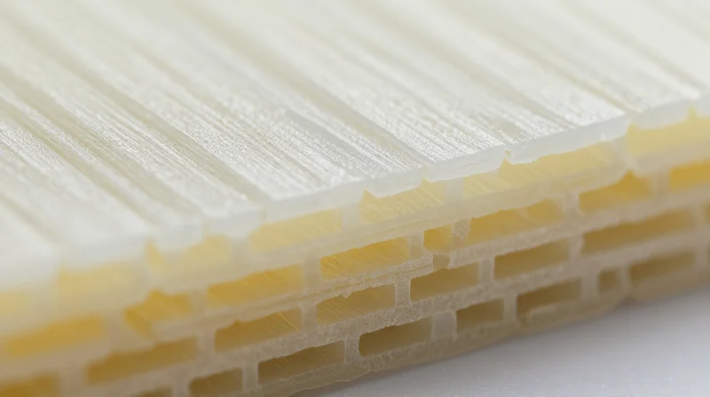
The Material Paradox of PTFE
PTFE-based laminates are favored in RF antenna applications for their exceptional dielectric stability and low dissipation factor. However, these same properties create inherent challenges during fabrication. Unlike rigid FR-4 substrates, PTFE is inherently soft, chemically inert, and sensitive to thermal processing, making standard mechanical drilling and etching processes ineffective or even destructive if not adapted for high-frequency performance requirements.
Comparative Analysis: FR-4 vs. PTFE
| Attribute | FR-4 (Standard) | PTFE (Teflon) |
|---|---|---|
| Mechanical Rigidity | High | Low (Flexible) |
| Dimensional Stability | Excellent | Poor (Prone to movement) |
| Chemical Reactivity | Reactive | Highly Inert |
| Thermal Expansion (Z-axis) | Low | High |
Key Fabrication Challenges
- How does PTFE's chemical inertness affect processing?
PTFE resists standard chemical desmear processes used to prepare holes for plating. Manufacturers must utilize specialized plasma etching techniques to modify the surface energy of the holes, enabling effective copper deposition. - What are the risks during mechanical drilling?
Due to its soft nature, PTFE can 'smear' during drilling, where the material melts and coats the drill bits. This requires low feed rates, specialized sharp bits, and precise speed control to prevent hole-wall contamination. - Why is registration difficult with PTFE?
PTFE substrates exhibit significant dimensional instability during thermal cycling. Material movement during the lamination and curing stages often necessitates oversized pads or compensation factors in the design phase to ensure accurate alignment.
Ignoring these unique physical characteristics often leads to plating voids, interconnect failure, and significant RF signal loss. Achieving manufacturing success with Teflon requires moving away from 'one-size-fits-all' DFM strategies and embracing specialized handling protocols tailored to high-frequency material science.
Critical Considerations for Copper Etching
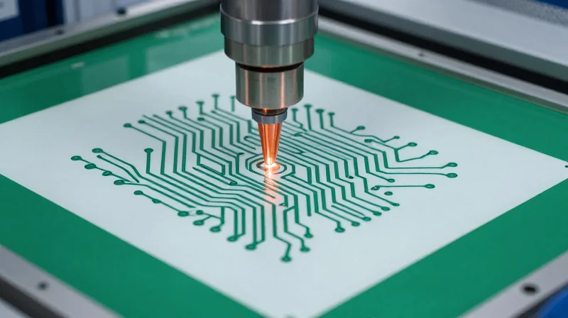
Copper etching on PTFE-based laminates is significantly more complex than standard glass-reinforced epoxies due to the non-polar, chemically inert nature of Teflon and its low surface energy. Failure to optimize the etching process leads to poor copper-to-dielectric adhesion or excessive undercut, both of which degrade signal integrity and shift characteristic impedance in high-frequency RF designs.
Mitigating Side-Etching for Impedance Control
Side-etching, or undercut, modifies the trapezoidal cross-section of copper traces, effectively altering the conductor width and increasing effective impedance. To maintain the tight tolerances required for microwave frequencies, manufacturers must implement specific controls:
- Etchant Chemistry
Utilize high-concentration cupric chloride or specialized alkaline etchants that offer a superior etch factor, allowing for thinner trace features with minimal lateral attack. - Spray Pressure Management
Lowering nozzle spray pressure prevents turbulence at the copper-dielectric interface, which is critical for maintaining vertical sidewalls on fine-pitch antenna geometries. - Conveyor Velocity
Optimize belt speed to balance throughput with residence time, ensuring that the etchant acts primarily on the copper thickness rather than eroding the trace width.
Comparison of Copper Bonding Treatments
| Treatment Type | Adhesion Strength | Impact on Skin Effect | Recommended Application |
|---|---|---|---|
| Mechanical Abrasion | Low | Minimal | Standard RF antennas |
| Chemical Etch-back | Medium | Moderate | High-reliability radar |
| Plasma Treatment | High | Low | Precision impedance |
Frequently Asked Questions
- Why does PTFE require specialized plasma treatment before metallization?
PTFE is chemically inert; plasma treatment increases surface wettability and creates microscopic anchor points, ensuring that the copper plating remains bonded through thermal cycling. - How does surface roughness impact RF performance?
Increased surface roughness increases the 'skin effect' losses, which raises insertion loss and alters the phase velocity, complicating impedance consistency at frequencies above 10 GHz.
Optimizing Laminating Techniques for Multi-Layer RF Boards

Optimizing Laminating Techniques for Multi-Layer RF Boards
Achieving reliable lamination in high-frequency Teflon PCB stacks requires a departure from standard epoxy-based methodologies. PTFE exhibits low surface energy and significant thermal expansion characteristics, demanding specialized bond-ply materials and precisely controlled pressure-temperature profiles to ensure uniform adhesion without compromising signal integrity.
Bond-Ply Selection and Material Compatibility
The mismatch between the Coefficient of Thermal Expansion (CTE) of rigid copper layers and the compliant nature of Teflon is the primary cause of delamination. Selecting a bonding material that bridges this gap while maintaining a low dielectric loss tangent is critical.
| Bonding Material Type | Key Advantage | Thermal Limitation |
|---|---|---|
| Fluorinated Ethylene Propylene (FEP) | Excellent electrical performance | Low melting point, potential flow issues |
| Modified PTFE / Thermoplastic | Higher process stability | Requires tighter pressure regulation |
| Pre-preg (Teflon-based) | Best material compatibility | Higher cost, sensitive to storage |
Thermal Cycle Management Protocols
Lamination of Teflon circuits is a time-temperature-pressure sensitive process. Rapid heating can cause material creep, while uneven cooling cycles introduce internal stresses that lead to warping or layer separation post-reflow.
- How do I mitigate internal stress during lamination?
Utilize a gradual ramp-up temperature profile and ensure the stack is cooled under uniform, sustained pressure to allow the bond-ply to polymerize evenly. - Why does pressure control matter for impedance?
Excessive pressure can cause the bond-ply to flow excessively, resulting in variations in the dielectric thickness which directly impacts the board's impedance profile. - Should I pre-bake the PTFE materials?
Yes, pre-baking is essential to remove absorbed moisture, which can cause outgassing and voids within the laminate interface during the high-temperature lamination cycle.
Drill Parameter Optimization for PTFE
Overcoming the Softness of PTFE
PTFE is inherently soft and thermally expansive, making it susceptible to resin smear and hole wall damage during the drilling process. Standard carbide drill bits designed for rigid FR-4 will cause tearing and nail-heading in PTFE. Successful fabrication requires high-quality, sharp drill bits—preferably with optimized geometry—and a strict adherence to specific speed and feed profiles to ensure smooth, debris-free hole walls.
Drill Geometry and Parameter Strategy
| Parameter | Recommendation for PTFE | Reasoning |
|---|---|---|
| Drill Bit Type | High-shear, polished carbide | Reduces friction and prevents heat buildup |
| In-feed Rate | Low to Moderate | Prevents mechanical stress and deformation |
| Surface Speed (SFM) | High (above 500 SFM) | Promotes clean cutting rather than rubbing |
| Retract Rate | High | Minimizes dwell time to prevent thermal smearing |
Operational Guidelines for Hole Quality
- How does drill bit sharpness impact PTFE boards?
A dull bit generates excessive frictional heat, leading to resin melt and smear, which complicates subsequent plating steps and can compromise signal integrity. - Why is entry/exit material critical?
Using phenolic or aluminum entry and exit material helps clamp the PTFE surface, preventing the drill from lifting the copper or tearing the soft dielectric layers during breakthrough. - Should I use peck drilling?
Peck drilling is generally discouraged for PTFE as it increases dwell time and mechanical wear; a single, continuous feed is preferred to maintain hole integrity.
Ultimately, the combination of a sharp, specialized tool geometry and a high-speed, low-chip-load approach is the industry standard for preventing the 'soft-state' deformation of Teflon. Always monitor the drill bit life carefully, as PTFE is significantly more abrasive to carbide than traditional glass-reinforced laminates, requiring more frequent tool changes to prevent wall defects.
Maintaining Surface Finish Quality

The Impact of Surface Roughness on Skin Effect
In RF antenna applications, the skin effect dictates that high-frequency currents concentrate at the conductor's surface. On Teflon substrates, microscopic copper roughness creates an effective path length longer than the physical trace dimension, drastically increasing signal attenuation and phase instability. Minimizing the root-mean-square (RMS) roughness of the copper foil is critical for maintaining consistent dielectric performance and minimizing insertion loss.
Selecting the Optimal Surface Finish
Surface finish selection for RF boards must balance solderability, oxidation resistance, and RF transmission characteristics. While traditional finishes like HASL are unsuitable for high-frequency applications, modern alternatives offer varying degrees of signal degradation based on their conductivity and layer thickness.
| Finish Type | RF Suitability | Key Advantage | Consideration |
|---|---|---|---|
| Immersion Silver | Excellent | Low cost, flat surface | Tarnish sensitivity |
| ENIG | Good | High reliability | Nickel is magnetic |
| ENEPIG | Very Good | Reduced signal loss | Complex process |
| ENEPIG / Gold | Optimal | High conductivity | Higher material cost |
Frequently Asked Questions
- Why is nickel problematic in high-frequency designs?
Nickel is ferromagnetic, which can cause parasitic inductive effects and increase signal loss at high microwave frequencies. - Does immersion silver provide better signal integrity than ENIG?
Generally yes, because immersion silver lacks the nickel layer, avoiding the magnetic skin effect issues prevalent in standard ENIG. - How does copper foil profile affect Teflon antenna performance?
A low-profile or 'VLP' (Very Low Profile) copper foil reduces the effective surface area for current flow, lowering resistive losses in high-frequency fields.
Thermal Management and Material Stability
PTFE-based materials offer exceptional electrical performance for RF antennas, but their high Coefficient of Thermal Expansion (CTE), particularly in the Z-axis, presents significant manufacturing challenges. Achieving dimensional stability requires a rigorous approach to stack-up design, lamination cycles, and thermal profile management to prevent registration errors and reliability failures.
Mitigating Z-Axis Expansion and Dimensional Drift
The primary issue with PTFE is its abrupt transition at the glass transition temperature (Tg), where expansion rates increase significantly. To mitigate registration drift during the reflow process, designers must prioritize balanced copper distribution across all layers to counteract structural warping.
| Parameter | PTFE Substrate | FR-4 (Standard) | Impact |
|---|---|---|---|
| CTE (Z-axis) | 150-300 ppm/°C | 30-50 ppm/°C | High risk of barrel cracking |
| Dimensional Stability | Lower | Higher | Requires registration compensation |
Design Guidelines for Thermal Reliability
- How does copper balance affect thermal stability?
Asymmetric copper distribution creates uneven thermal stress, causing the PCB to warp during thermal cycling. Maintain a symmetrical stack-up with equal copper weight and density on opposing layers. - Can I use standard vias on PTFE PCBs?
Due to the high Z-axis expansion, standard vias are prone to fracture. Use reinforced or filled via structures, and minimize aspect ratios to reduce stress on the hole wall-to-pad interface. - What role does lamination pressure play?
Precise control of lamination pressure is critical to prevent 'flowing' of the dielectric. Over-pressurization can cause substrate deformation, resulting in impedance mismatches.
Ultimately, success with Teflon RF PCBs hinges on coordinating with your fabrication partner to verify that pre-preg materials and foil treatments are compatible with your specific thermal assembly profile. Designing for the material's inherent instability rather than fighting it is the cornerstone of DFM excellence.
Testing Protocols for Signal Integrity Verification

Verification Framework for RF Signal Integrity
Verifying Teflon-based PCB designs requires a dual-pronged approach focusing on Time Domain Reflectometry (TDR) for impedance discontinuity analysis and Vector Network Analysis (VNA) for frequency-domain performance. Because PTFE substrates exhibit unique mechanical and dielectric properties, testing protocols must specifically account for the sensitivity of the signal path to etching variances and layer-to-layer registration.
Core Testing Methodologies
| Methodology | Target Metric | Key DFM Insight |
|---|---|---|
| TDR Analysis | Characteristic Impedance | Identify discontinuities at vias or pad transitions. |
| VNA Sweep | Return/Insertion Loss | Validate S-parameters against simulation models. |
| Micro-sectioning | Trace Geometry | Verify etching profiles and copper roughness. |
Frequently Asked Questions on RF Testing
- Why is TDR critical for Teflon RF boards?
Teflon substrates are prone to impedance shifts during fabrication due to slight variations in dielectric constant or copper thickness; TDR pinpoints these physical locations for immediate corrective action. - How does surface roughness impact VNA results?
Increased surface roughness on copper layers leads to higher insertion loss at millimeter-wave frequencies due to the skin effect, often requiring surface finish selection based on VNA validation rather than just chemical compatibility. - Should I include test coupons in my DFM panel?
Yes, implementing identical-construction test coupons allows for non-destructive verification of impedance profiles without sacrificing the production antenna, providing a reliable proxy for signal integrity.
Final verification should correlate VNA measurements directly with the original simulation files. If discrepancies exceed 1.5 dB at the operating frequency, conduct a microscopic investigation of the trace width and dielectric spacing to ensure the manufacturing process has maintained the intended design constraints.
Achieving excellence in RF antenna fabrication requires a deep synergy between design intent and manufacturing capability. By adhering to these rigorous DFM protocols, engineers can minimize signal loss and maximize reliability. Ready to optimize your high-frequency designs? Contact our engineering team today for a DFM review of your latest RF project.
