
In the fast-evolving landscape of Industrial IoT, the performance of your LoRaWAN gateway is only as reliable as its PCB design. High-frequency RF environments demand precision; even minor layout errors can lead to devastating signal degradation. This guide distills twenty years of engineering expertise into actionable DFM rules, empowering you to move from prototype to robust, large-scale industrial deployment without compromising signal integrity or thermal stability.
The Anatomy of a High-Performance RF PCB
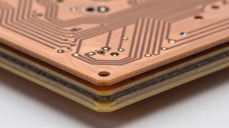
Substrate Selection: FR4 vs. High-Frequency Laminates
The choice of dielectric material is the foundational decision in RF PCB design. While FR4 is cost-effective, its inconsistent dielectric constant (Dk) and high dissipation factor (Df) can cause significant signal degradation in sensitive RF front-end circuits. For LoRaWAN gateways operating in the 868MHz or 915MHz bands, transitioning to high-frequency laminates like Rogers or specialized Teflon-based materials is often necessary to minimize loss and maintain impedance stability.
| Material Property | Standard FR4 | Rogers 4000 Series |
|---|---|---|
| Dielectric Constant (Dk) | 4.2 - 4.8 (Inconsistent) | 3.48 - 3.66 (Stable) |
| Dissipation Factor (Df) | 0.020 | 0.0037 |
| Cost Profile | Low | High |
| Application | Low-speed digital | RF Front-ends / LoRa |
Impact of Dielectric Constant on Signal Propagation
The dielectric constant directly influences the propagation velocity of electromagnetic waves. In RF PCB traces, the Dk dictates the effective wavelength of the signal, which directly impacts the accuracy of microstrip and stripline impedance calculations. Any variation in Dk—whether due to manufacturing tolerances or temperature fluctuations—will shift the impedance of your RF traces, resulting in return loss and reduced sensitivity for your gateway.
Technical Considerations for RF Layout
- Why is impedance matching critical?
Mismatched impedance leads to signal reflections that degrade the Power Added Efficiency (PAE) of the gateway transmitter and introduce noise in the receiver. - How does substrate thickness affect performance?
Thinner substrates allow for narrower traces while maintaining a 50-ohm impedance, which is beneficial for miniaturizing complex RF circuitry near the antenna connector. - Is moisture absorption a concern?
Yes, FR4 absorbs moisture significantly more than high-frequency laminates, which can shift the Dk value over time and lead to field-performance degradation in humid environments.
Mastering Impedance Control in LoRaWAN Layouts
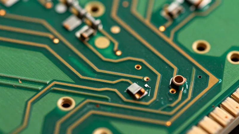
Achieving 50-Ohm Trace Impedance
To maintain a 50-ohm characteristic impedance in LoRaWAN layouts, you must calculate trace width based on the dielectric constant (Dk) of your substrate, the height of the dielectric layer above the ground plane, and the copper thickness. Microstrip lines are the industry standard for top-layer RF routing, but you must ensure a continuous, low-impedance return path directly beneath the signal line.
| Parameter | Effect on Impedance | Design Mitigation |
|---|---|---|
| Trace Width | Increase decreases impedance | Use a PCB impedance calculator |
| Dielectric Height | Increase increases impedance | Keep RF layers close to GND |
| Copper Thickness | Increase decreases impedance | Standardize for manufacturing |
Minimizing Parasitic Capacitance and Inductance
Parasitic components are the silent killers of RF performance in LoRaWAN gateways. At 868/915 MHz, vias act as inductors and large solder pads create parasitic capacitance, both of which introduce discontinuities in the transmission line. To mitigate these effects, implement via stitching around your RF traces and keep ground pours as close to the trace as possible without compromising clearance rules.
Key Impedance Control FAQ
- Why is a continuous ground plane essential?
A continuous ground plane provides the shortest return path for high-frequency current, minimizing loop area and preventing signal radiation or unwanted electromagnetic coupling. - How do I handle layer transitions?
If you must transition between layers, use at least two ground stitching vias placed as close to the signal via as possible to maintain a constant reference plane and minimize parasitic inductance. - Does solder mask impact impedance?
Yes, solder mask increases the effective dielectric constant of the surface, which can shift the impedance by 2-5 ohms; always factor in solder mask thickness when calculating trace widths.
// Impedance optimization rule for microstrip
// Width = 0.5 * (50 ohm target constraint)
// Ensure no ground plane cutouts beneath RF traces
VOID_RF_PLANAR_DISCONTINUITY = True;
MIN_VIA_STITCHING_SPACING = "1.5mm";
Minimizing Signal Loss: Grounding and Shielding Strategies
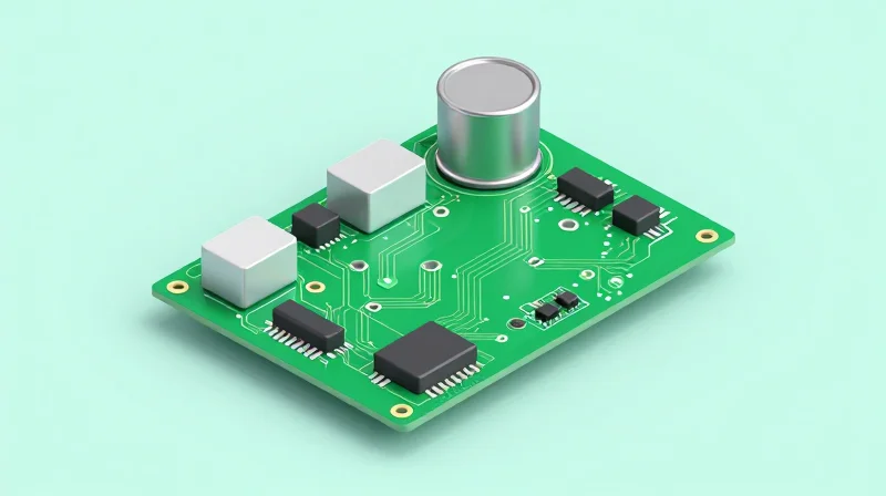
Unified Ground Plane Architecture
The foundation of a low-noise LoRaWAN PCB is a solid, contiguous ground plane that serves as the return path for all high-frequency signals. Fragmentation of the ground plane via excessive component cutouts or signal routing causes ground bounce and induces return current loops, which directly degrade signal integrity and increase electromagnetic emissions.
Isolation Techniques for Mixed-Signal Domains
Maintaining spatial separation between digital processing units and the RF analog front-end (AFE) is critical. Use the following shielding and layout practices to prevent noise coupling:
- Component Partitioning
Physically separate the microcontroller and high-speed digital interfaces from the LoRa transceiver by at least 15-20mm. - Via Stitching
Employ a dense array of ground vias (stitching vias) along the perimeter of the RF section to suppress edge radiation and contain internal field resonance. - Faraday Cages
Utilize dedicated metal RF shields soldered onto the PCB over the RF circuitry to block both radiated and near-field interference from digital clocks and power switching circuits.
Comparative Analysis: Shielding and Grounding Strategies
| Method | Primary Benefit | Implementation Tip |
|---|---|---|
| Solid Ground Plane | Controlled return paths | Avoid splitting under RF signal traces |
| Via Stitching | Reduces EMI/RFI radiation | Ensure spacing is |
| Metal Shield Cans | Prevents external coupling | Ensure low-impedance ground contact points |
Critical Design Guidelines
When placing vias, prioritize proximity to signal transitions. A return current path that deviates from the signal trace increases inductance, creating a loop antenna that emits noise. Always place a dedicated ground via immediately adjacent to any signal via that transitions layers.
Thermal Dissipation Techniques for Industrial Reliability

Managing Heat in Constrained Industrial Enclosures
In industrial LoRaWAN gateways, ambient temperatures combined with high-density component integration often lead to thermal throttling or premature component failure. To ensure reliability, designers must treat the PCB as a primary heat sink, utilizing controlled copper pours and strategic component placement to shunt heat away from sensitive RF front-end modules and high-speed processors toward the enclosure chassis.
Thermal Vias and Copper Pour Strategies
Thermal vias serve as the vertical conduit for heat transition between PCB layers. By implementing an array of vias directly under thermal pads—filled and capped if necessary for solder mask consistency—the board effectively acts as an extended heat spreader. Connecting these vias to substantial internal ground planes or external heat-sinking copper areas increases the effective thermal mass of the design.
| Technique | Primary Benefit | Implementation Tip |
|---|---|---|
| Thermal Vias | Conducts heat to internal layers | Use 0.3mm diameter for optimal plating ratio. |
| Copper Pours | Increases total thermal mass | Tie to ground plane for EMI shielding and heat spreading. |
| Component Isolation | Prevents localized hotspots | Separate high-power DC-DC converters from RF chains. |
Frequently Asked Questions on Thermal Reliability
- How many thermal vias are enough?
While a specific number depends on the power dissipation (W), a grid of 0.3mm vias spaced 0.8mm to 1.0mm apart under high-power components generally provides sufficient dissipation without compromising structural integrity. - Does solder mask affect thermal dissipation?
Yes, standard solder mask acts as a thermal insulator. For high-power RF components, consider exposing the copper on the bottom side of the PCB and using a high-conductivity thermal interface material (TIM) to bridge the gap to the metal enclosure. - Should I use internal or external layers for heat dissipation?
External layers are preferred if they can be coupled to a chassis heat sink; however, internal ground planes provide a more uniform distribution of heat across the board, reducing local stress on sensitive components.
Antenna Placement and Near-Field Coupling
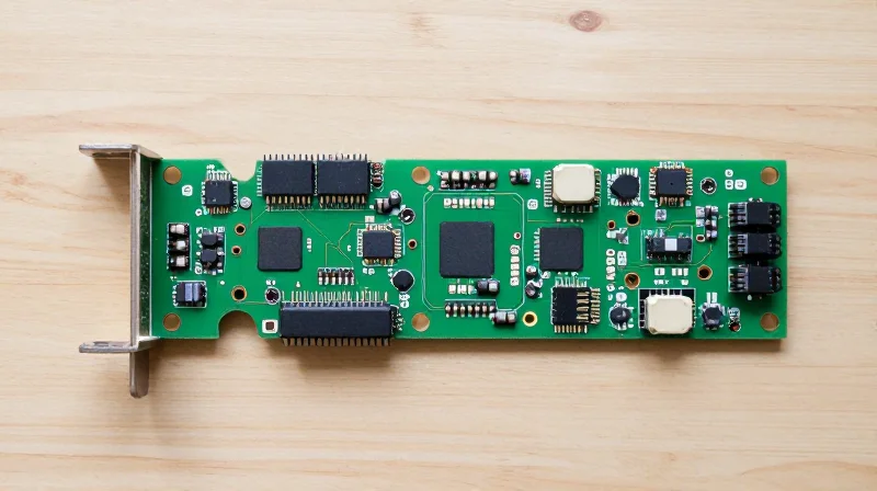
Strategic Antenna Placement for Maximum Link Budget
Antenna placement is the single most critical factor in LoRaWAN gateway performance. The antenna connector should be positioned at the board edge to ensure a clear aperture for radiation. Keeping the RF launch point away from internal high-frequency switching noise and bulky components like power inductors is essential to avoid pattern distortion and localized desensitization.
Preventing Near-Field Coupling
Near-field coupling occurs when magnetic or electric fields from digital traces induce currents in the sensitive RF input stage. To maintain signal integrity, follow these isolation guidelines:
- Trace Orientation
Route high-speed digital clocks or data buses perpendicularly to RF traces to minimize electromagnetic induction. - Isolation Trenches
Use 'moats' or copper keep-out zones between the RF section and the digital processing core to break return path coupling loops. - Shielding Can placement
Place an RF shield directly over the LoRa transceiver and its matching network, ensuring the ground pins are stitched to the PCB ground plane every 3-5mm.
Comparative Impact of Design Choices
| Design Practice | Impact on RF Performance | Risk Level |
|---|---|---|
| U.FL edge mount | Minimal insertion loss | Low |
| Digital traces under RF | High noise injection | Critical |
| Solid ground plane stitching | Improved return loss | Low |
Common Implementation FAQs
- How far should I keep digital components from the antenna feed?
Maintain a minimum distance of at least 15mm to 20mm from any high-frequency digital clock sources or switching regulators. - Does the enclosure material affect placement?
Yes; metal enclosures require bulkhead connectors and external antennas, while plastic housings allow for internal PCB-trace antennas, provided the dielectric constant of the plastic is accounted for.
DFM Rules for Scalable Manufacturing
Standardizing PCB Geometry and Fabrication Constraints
To achieve high-volume manufacturing success, designers must implement a strictly defined set of geometric constraints. Uniformity across trace widths and pad geometries reduces the potential for acid traps and plating variations during the etching process, which are frequent causes of open or short circuits in complex RF designs.
| Feature | Standard Industrial Spec | RF Optimized Spec |
|---|---|---|
| Minimum Trace/Space | 5 mil / 5 mil | 6 mil / 6 mil (to reduce edge roughness) |
| Annular Ring | 3 mil | 5 mil (for structural via integrity) |
| Solder Mask Clearance | 3 mil | 4 mil (to prevent registration encroachment) |
Preventing Assembly Defects: Best Practices
- How does copper balancing affect PCB warping?
Asymmetric copper distribution leads to thermal expansion differences during reflow. Always ensure that ground and power pours are balanced across both sides of the board to maintain structural flatness. - Why is thermal relief mandatory for via-in-pad structures?
Direct connection to large copper planes acts as a heat sink, leading to cold solder joints. Use thermal relief spokes for all through-hole connections unless high-current paths dictate direct thermal connection. - What is the role of fiducial markers in assembly?
Precision placement of at least three global fiducials and local fiducials for fine-pitch BGA components is essential for automated optical inspection (AOI) and high-accuracy surface mount machine alignment.
Optimizing Solder Mask and Silkscreen
For LoRaWAN gateways, solder mask defined pads are recommended for high-reliability components to prevent solder migration. Furthermore, ensure that silkscreen markings are clipped away from solder pads by at least 10 mils; failure to do so results in 'solder bridging' where the mask ink prevents proper solder wetting during the reflow process.
Testing and Verification Protocols for RF Compliance
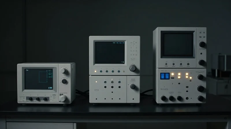
Validation of RF Performance and Compliance
Post-fabrication verification is the final safeguard against field failures. By implementing a structured testing regime, you ensure that the actual performance of your LoRaWAN gateway matches the theoretical models defined during the layout phase.
Essential Measurement Protocols
| Measurement Type | Tool Required | Primary Objective |
|---|---|---|
| Return Loss (S11) | Vector Network Analyzer (VNA) | Validate antenna impedance matching at 868/915 MHz. |
| Conducted Power | Spectrum Analyzer | Ensure output power complies with regional EIRP limits. |
| Harmonic Emissions | Spectrum Analyzer | Check for spurious emissions exceeding regulatory thresholds. |
Verification FAQ
- Why is VNA testing critical for the antenna path?
The VNA identifies impedance mismatches caused by manufacturing tolerances or parasitic capacitance, which directly influence range and link budget. - How do you handle slight deviations in resonant frequency?
If the resonance shifts, implement a Pi-matching network on the PCB layout to allow for post-assembly fine-tuning of the antenna impedance. - Is chamber testing necessary for LoRaWAN gateways?
Yes, radiated emissions testing in an anechoic chamber is essential to verify that the enclosure and PCB integration do not create unexpected interference patterns.
Compliance Documentation
Maintain a 'Golden Sample' record. Once a design is verified and passes FCC or CE compliance, use that specific unit as the benchmark for all future production batches. Automated Optical Inspection (AOI) should be programmed to verify that the impedance-critical components, such as matching inductors and capacitors, are identical to the verified unit.
Navigating Supply Chain Constraints in PCB Production
Strategic Component Selection for Resilience
The key to resilient LoRaWAN gateway production lies in adopting a 'design-for-availability' mindset. By selecting components with multiple drop-in equivalents and avoiding single-source proprietary RF chips, you mitigate the risk of assembly halts due to localized shortages. Focus on standard package sizes (e.g., 0402 or 0603 for passives) and widely supported microcontrollers that maintain compatibility across various supply nodes.
Material Standardization and EMC Integrity
Substituting materials often jeopardizes electromagnetic compatibility (EMC). To maintain your design integrity during supply constraints, specify standard FR-4 laminates with known dielectric constants, ensuring that any material substitution undergoes a comparative analysis of the dissipation factor and moisture absorption to preserve the RF transmission characteristics required for LoRaWAN gateway performance.
| Constraint Factor | Strategy for Mitigation | Impact on Performance |
|---|---|---|
| Active Component Shortage | Pin-compatible second-sourcing | Minimal if PCB footprint is shared |
| Substrate Availability | Standardize to high-Tg FR-4 | Predictable signal integrity |
| Passives Lead Times | Use common 0402/0603 footprints | Zero impact on design specs |
Supply Chain FAQs
- How can I avoid redesigns when specific RF components are unavailable?
Design your PCB footprints to accommodate multiple manufacturers' parts by adhering to universal land pattern standards, such as those defined in IPC-7351. - Does changing the PCB laminate affect my RF compliance?
Yes, variations in the dielectric constant (Dk) will shift your impedance-controlled traces. Always re-simulate or test with VNA if the Dk varies by more than 0.05 from the original design baseline. - Is it better to stock parts or change the design?
For high-volume LoRaWAN production, forward-buying long-lead-time silicon is generally more cost-effective than the time and compliance costs associated with re-certifying a revised board design.
Achieving industrial-grade reliability for LoRaWAN gateways requires a holistic approach that balances RF physics with practical assembly requirements. By implementing these advanced DFM strategies, you can eliminate bottlenecks and ensure your hardware stands up to the most demanding environments. Are you ready to elevate your hardware design process? Contact our engineering team today for a comprehensive design review of your next IoT project.
