Mastering PCB Design: A Comprehensive Guide for Beginners to Experts
2025.01.18
From the smartphone in your pocket to the complex systems powering our world, Printed Circuit Boards (PCBs) are the unsung heroes of modern electronics. This guide demystifies PCB design, transforming the seemingly daunting process into a clear, step-by-step journey. We'll explore everything from the fundamental concepts to advanced techniques, equipping you with the knowledge and skills to design your own PCBs with confidence. Whether you're a beginner eager to learn or an experienced engineer seeking to refine your craft, this is your one-stop resource for mastering the art of PCB design.
Understanding the Fundamentals of PCB Design
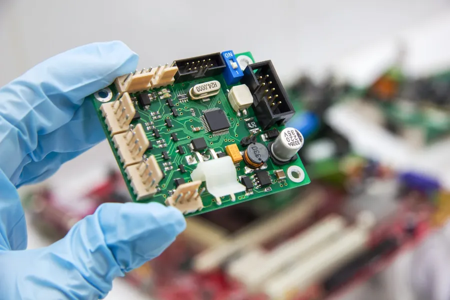
Printed Circuit Board
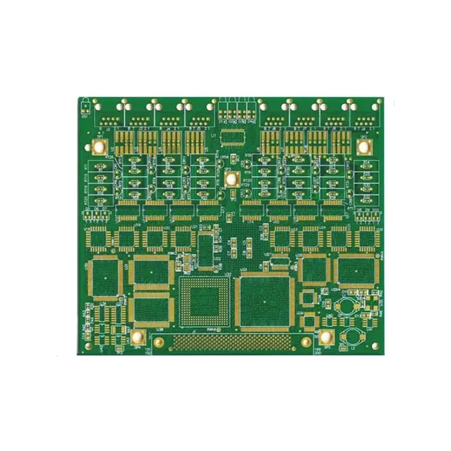
Printed Circuit Boards (PCBs) are the foundational building blocks of nearly all electronic devices, serving as the physical platform to support and connect electronic components. This section will delineate the core principles of PCB design, encompassing what PCBs are, their constituent elements, and their crucial role in electronic systems, while clarifying essential terminology, such as layers, vias, and traces.
A PCB's primary function is to provide mechanical support and electrical connections for electronic components. Rather than relying on haphazard wiring, PCBs utilize conductive pathways, commonly etched from copper, to create a structured, durable, and reliable assembly. This approach allows for the mass production and efficient assembly of complex electronic circuits.
Layers PCBs are composed of one or more layers, each containing conductive pathways. Single-layer PCBs are used for simpler designs, while multi-layer PCBs enable more intricate circuits. Layers can be dedicated to power, ground, and signals. The number of layers affects the board's signal routing capacity and overall complexity.
Traces Traces are conductive pathways, typically made of copper, that serve as wires on the PCB. The width and spacing of traces are critical design considerations that determine their current-carrying capacity and impedance, which are important factors in circuit performance.
Vias Vias are holes in the PCB used to create electrical connections between different layers. They can be through-hole (connecting all layers), blind (connecting one outer layer to an inner layer), or buried (connecting two or more inner layers). The size and number of vias are important parameters to ensure good connections across layers.
Pads Pads are conductive areas on the surface of the PCB where components are soldered. They come in different shapes and sizes, depending on the component type, such as surface-mount device (SMD) pads or through-hole pads.
Schematic Capture: The Blueprint of Your PCB
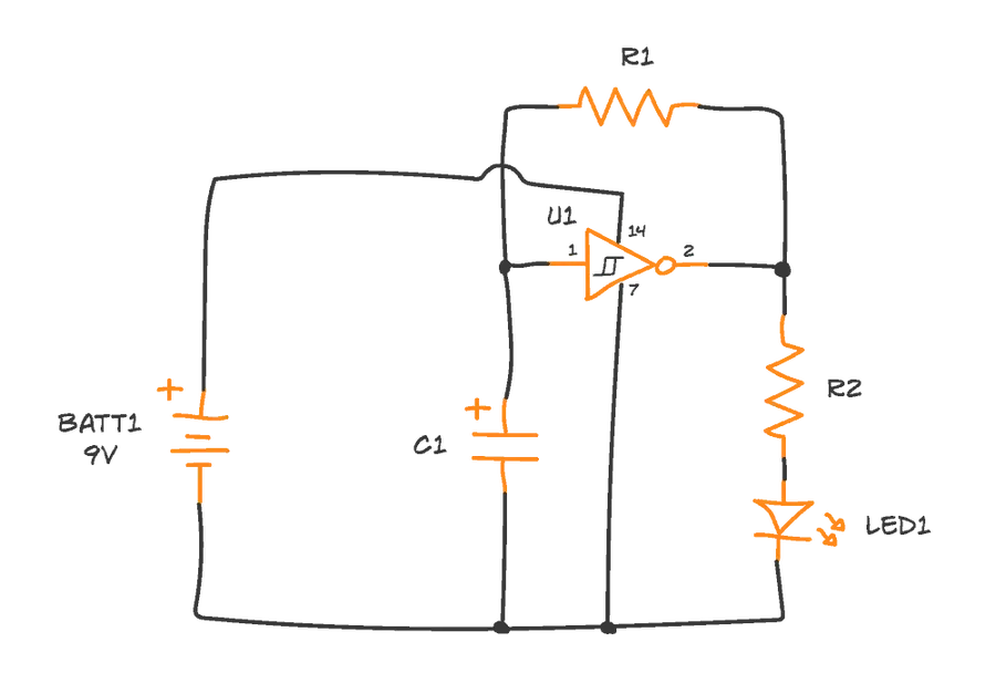
Circuit Schematic
Schematic capture is the critical initial phase in PCB design, involving the creation of a circuit diagram that visually represents the electronic connections within your design. This schematic serves as the blueprint for the physical PCB layout and is essential for accurate and successful board fabrication.
This process employs specialized software to select components, connect them logically and accurately, define nets, and finally prepares the design for the subsequent layout phase. A meticulous schematic ensures a trouble-free transition into PCB layout, minimizing the risk of errors and iterations later.
Component Selection: Selecting the correct components is fundamental. Ensure that the chosen parts meet the design specifications regarding voltage, current, tolerance, and other relevant parameters, based on a thorough review of datasheets.
Net Connections: Accurately connecting the component pins is necessary to establish the correct electrical paths as specified in the circuit design. Pay close attention to the correct polarity and logical connections. Mislabeled or incorrect connections will result in a nonfunctional PCB.
Preparation for Layout: The final stage of schematic capture involves preparing the design for physical layout by assigning component footprints, specifying design rules and verifying electrical rule checks (ERCs) to uncover any potential errors.
PCB Layout: From Diagram to Physical Board
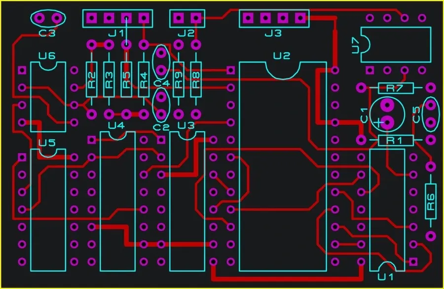
PCB Layout Software
Transforming a schematic diagram into a functional physical printed circuit board (PCB) layout is a critical step in electronics design. This process involves strategically arranging components and creating conductive pathways (traces) on the board, ensuring signal integrity, manufacturability, and optimal performance.
Key considerations include component placement, routing strategies, thermal management, and adherence to design rules and constraints for manufacturing.
Component Placement Strategic placement of components to minimize routing distance, reduce signal interference, and optimize thermal performance. Factors include component size, heat dissipation requirements, and signal flow.
Routing Techniques Creating conductive traces to connect components according to the schematic. This involves selecting appropriate trace widths, clearances, and layer assignments, employing techniques like differential pair routing and impedance control for signal integrity.
Optimization for Signal Integrity Ensuring that signals propagate accurately and without degradation by addressing impedance matching, minimizing signal reflections, and reducing crosstalk. This also includes implementing strategies for noise reduction, such as proper grounding and decoupling.
Manufacturability Considerations Designing the PCB layout with manufacturing capabilities and constraints in mind. This involves adhering to minimum trace width, spacing, and via size, and employing best practices to avoid manufacturability issues.
Aspect
Description
Impact
Component Placement
Arrangement of components on the board
Affects routing efficiency, signal integrity, and thermal management
Routing
Creation of conductive paths connecting components
Determines signal quality, current handling capacity, and manufacturing feasibility
Signal Integrity
Maintaining signal quality during transmission
Ensures proper circuit operation and prevents signal loss or distortion
Manufacturability
Design aspects ensuring ease of fabrication and assembly
Reduces manufacturing costs and increases board reliability
Choosing the Right PCB Design Software
PCB Design Software Interface
Selecting the appropriate PCB design software is crucial for a successful project, impacting efficiency, cost, and the final product's quality. This section provides a comparative analysis of leading software options, guiding you through their features, usability, cost implications, and suitability for different project types. The ultimate choice should align with your specific needs, design complexity, budget, and technical expertise.
The primary considerations when selecting PCB design software include functionality, user interface, cost, and the learning curve.
Key Features to Consider Evaluate software based on schematic capture, PCB layout, simulation, and collaboration capabilities.
User Interface and Usability Prioritize software with an intuitive design and efficient workflow to minimize the learning curve and design time.
Cost Implications Consider both initial purchase costs and ongoing subscription fees, as well as any additional costs for libraries and support.
Scalability for project complexity Ensure the software can handle your projects' current and future complexity, including the number of layers, components, and high-speed design requirements.
Library Management A software's component library is critical and needs to be extensive, easily manageable and allow custom creation.
PCB Design Software Comparison
Selecting the appropriate PCB design software is crucial for a successful project. This section provides a comparative analysis of leading PCB design software platforms, highlighting their key features, pricing structures, and usability to aid in making an informed decision tailored to your specific project requirements.
Software
Key Features
Price
Usability
Project Suitability
Altium Designer
Comprehensive feature set, advanced routing capabilities, robust simulation tools, strong data management, extensive component library, collaborative design features
High (Subscription-based)
Complex, with a steep learning curve, but powerful for advanced users
Ideal for complex, high-density, and high-speed designs; suitable for professional engineering teams.
EasyEDA
Cloud-based, easy-to-use interface, large community library, integrated order system, basic simulation capabilities
Free for basic use, subscription options for enhanced features
User-friendly with a relatively short learning curve, accessible for hobbyists and beginners
Good for hobbyist projects, simple to medium complexity designs, and rapid prototyping.
KiCad
Open-source, free to use, cross-platform, growing library support, good simulation capabilities
Free
Moderate learning curve, but powerful for its price, suitable for intermediate to advanced users
Suitable for a wide range of projects from hobbyist to professional, good for users who prefer open-source solutions.
Autodesk Fusion 360
Cloud-based, integrated CAD/CAM/CAE, PCB design, mechanical integration, simulation features
Subscription-based, with educational licenses
Moderate learning curve; unified design environment, beneficial for mechanical and electrical integration.
Best for projects requiring both mechanical and electrical design integration; useful for product development cycles.
Advanced PCB Design Techniques
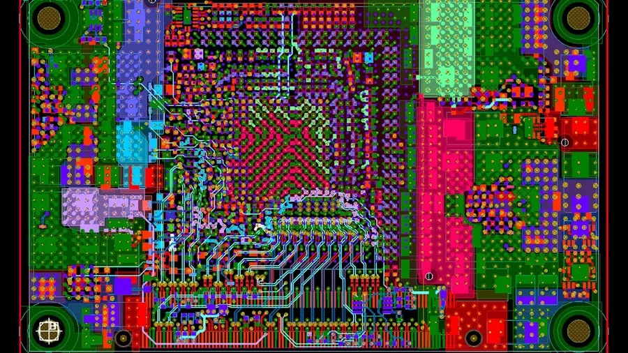
Multilayer PCB
Mastering advanced PCB design techniques is crucial for creating high-performance and reliable electronic products. This section explores impedance matching, differential pair routing, and high-speed design considerations, emphasizing their impact on signal integrity and overall system performance.
Impedance Matching Ensures maximum power transfer and minimizes signal reflections by matching the impedance of the source, transmission line, and load. Mismatched impedances can lead to signal distortion and reduced efficiency. Controlled impedance traces and specific stack-ups are key to achieving impedance matching.
Differential Pair Routing Involves routing two traces in parallel to carry complementary signals. This technique improves noise immunity and reduces electromagnetic interference (EMI), critical for high-speed data transmission. Careful attention to length matching and spacing is required.
High-Speed PCB Design Considerations Focuses on addressing the unique challenges of routing signals with fast rise times and high frequencies. This includes considerations such as signal integrity, crosstalk, EMI reduction, and power distribution network (PDN) design. Proper stack-up design, trace geometries, and termination techniques are essential.
Technique
Description
Key Considerations
Benefits
Impedance Matching
Matching impedance between source, trace, and load.
Controlled trace impedance, stack-up design.
Maximum power transfer, minimizes signal reflections.
Differential Pair Routing
Routing two traces in parallel for complementary signals.
Length matching, controlled spacing between traces.
Enhanced noise immunity, reduced EMI.
High-Speed Design
Addressing challenges of high-frequency signal routing.
Signal integrity, crosstalk, PDN design, EMI reduction.
Reliable signal transmission, optimum circuit performance.
PCB Manufacturing Process: From Design to Reality
PCB Manufacturing
The journey from a finalized PCB design to a tangible circuit board involves a complex sequence of manufacturing processes. This section elucidates the key stages of PCB manufacturing, encompassing fabrication, assembly, and testing, with a critical focus on design for manufacturability (DFM) considerations to ensure a seamless transition from design to physical product.
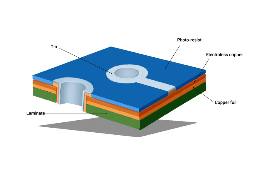
PCB fabrication is the core process where the physical board is created. It starts with the design data, which are used to generate the necessary artwork for each layer of the PCB. The process includes several key steps:
Inner Layer Imaging A photosensitive film is applied to copper clad laminate, exposed to UV light through a film mask to transfer the desired circuit patterns, and then chemically etched to remove unwanted copper. This step is repeated for each inner layer.
Layer Lamination The inner layers are carefully stacked with prepreg (a semi-cured epoxy resin) and copper foil, aligned, and then subjected to heat and pressure, bonding them together into a single multilayer structure.
Drilling Precision drilling creates holes for vias (interlayer connections) and component leads. These holes are drilled using numerically controlled machines with small drill bits, and accuracy is critical for proper connection and functionality.
Plating After drilling, the board undergoes a plating process to deposit copper within the drilled holes, establishing conductive connections between layers. This is an essential part of the process for creating vias.
Outer Layer Imaging and Etching Similar to inner layer processing, the outer layers are imaged and etched to define the traces, pads, and other features on the top and bottom surfaces of the board.
Solder Mask Application A layer of solder mask is applied to protect the copper traces from oxidation and prevent solder bridging during the assembly process. This mask is selectively applied, leaving the solder pads exposed.
Silkscreen Printing Finally, silkscreen printing applies component designators and other identifying information onto the board using a non-conductive ink. This is crucial for proper assembly.
Surface Finish A surface finish (such as HASL, ENIG, or OSP) is applied to the exposed copper pads to protect them from oxidation and ensure good solderability. The choice of surface finish depends on the application requirements.
Following fabrication, the PCB assembly process begins, which is the attachment of electronic components to the bare PCB. Key stages include:
Solder Paste Application Solder paste, a mixture of solder particles and flux, is applied to the component pads of the PCB. This is usually done with a stencil and automated screen printing, or a robotic solder paste dispenser.
Component Placement Components are picked from reels or trays and accurately placed onto the PCB pads using automated pick-and-place machines according to the component location data.
Reflow Soldering The assembled board is passed through a reflow oven where the solder paste melts and solidifies, creating a permanent electrical and mechanical connection between components and the board.
Inspection Automated optical inspection (AOI) and X-ray inspection are often used to check the quality of the solder joints and identify any defects.
After assembly, PCBs undergo rigorous testing to ensure they meet design specifications. Common testing methods include:
In-Circuit Testing (ICT) ICT uses test points to check the proper connection and function of individual components on the board. This is important to identify any component level failures.
Functional Testing Functional testing simulates real-world operating conditions to verify that the assembled PCB performs according to its intended function. This ensures overall board functionality.
Design for Manufacturability (DFM) is paramount in PCB design. This means taking into account the manufacturing constraints and capabilities during the design phase. DFM helps ensure a smooth transition to the physical realization of the PCB, reducing potential problems, improving product reliability, and reducing manufacturing costs. Key DFM considerations include:
Trace Width and Spacing Ensuring minimum trace width and spacing requirements are met for the manufacturing process and the voltage/current requirement. Incorrect design in this can result in manufacturing defects.
Via Placement Proper via placement helps with manufacturability and signal integrity. Poor placement can cause problems in manufacturing such as shorts or opens.
Component Footprints Using appropriate component footprints ensures correct part placement and soldering. Incorrect footprint can result in costly rework.
Panelization Optimizing board panelization to fit the manufacturing process and reduce material waste during production. Proper panelization can significantly reduce cost.
Solder Mask and Silkscreen Providing appropriate clearance around the pads. Ensure clear silkscreen and solder mask openings to avoid production issues.
Frequently Asked Questions About PCB Design
This section addresses common queries surrounding PCB design, providing clear and concise answers to help both beginners and experienced individuals understand key aspects of this field. We aim to clarify the fundamental concepts, learning curves, and career prospects related to PCB design.
What exactly is PCB design? PCB (Printed Circuit Board) design is the process of creating the physical layout of electronic circuits. It involves arranging electronic components on a board and creating conductive pathways (traces) that connect them. This process translates electronic schematics into a physical format suitable for manufacturing.
Is PCB design difficult to learn? The difficulty of learning PCB design depends on individual aptitudes and dedication. While the fundamental principles can be grasped relatively quickly, mastering advanced techniques requires time and practice. The learning curve can be steep initially, particularly when starting with complex software and intricate design methodologies, but with consistent effort, anyone can develop proficiency. Focus on building a strong foundation in electronics and computer-aided design (CAD) principles.
Can I learn PCB design independently? Yes, you can absolutely learn PCB design on your own. Numerous resources are available online, such as tutorials, courses, and open-source tools. However, while self-learning offers flexibility, it often requires a high level of self-discipline and may take longer to grasp advanced nuances compared to a structured educational path. Start with basic tutorials and gradually delve into complex areas, practice frequently and don't hesitate to seek help from online communities.
What is a typical salary for a PCB designer? The salary of a PCB designer varies greatly based on experience, location, and the complexity of the projects. Entry-level positions might start at a modest rate, but experienced designers with advanced skills in high-speed design or specific industry applications can command significantly higher salaries. Compensation can range from around $50,000 annually for beginners, to over $150,000 for experienced and specialized professionals. The demand for skilled PCB designers, especially those with expertise in high-frequency design, is continually growing, driving competitive compensation packages.
What are the key skills needed for PCB design? Key skills include a solid understanding of electronic circuit theory, proficiency in using CAD software (such as Altium Designer, KiCad, or Eagle), strong problem-solving abilities, attention to detail, and familiarity with manufacturing processes. Also, developing a deep comprehension of signal integrity, power management, and electromagnetic compatibility (EMC) is essential for complex designs. A willingness to learn continuously is also important, as this field is constantly evolving due to new technologies and manufacturing techniques.
How long does it take to become proficient in PCB design? Proficiency in PCB design depends heavily on individual learning pace and dedication. A basic understanding and some initial skills can be developed in a few months of consistent learning and practice. However, achieving a professional level, able to manage complex and critical PCB designs, typically requires 1-3 years of continuous experience and learning. This includes understanding advanced concepts, signal integrity, power management, and best practices for manufacturability. Experience gained through hands-on projects and diverse applications is paramount to achieving true mastery.
What are some common mistakes beginners make in PCB design? Common mistakes include neglecting design rule checks (DRC), improper component placement that compromises functionality or manufacturability, inadequate routing leading to signal integrity issues or crosstalk, ignoring impedance matching, and lack of attention to thermal management. Often overlooking design for manufacturability (DFM) results in boards that are difficult or expensive to produce. New designers should also ensure their understanding of grounding principles and decoupling, as poorly executed power distribution networks are a significant source of problems. Regularly checking and refining your design based on feedback is essential for avoiding common pitfalls and achieving a good quality design.
Tips for Effective PCB Design
Effective PCB design hinges on a meticulous approach, combining strategic component selection, optimized layout techniques, and rigorous error checking. Avoiding common pitfalls through a deep understanding of best practices can significantly improve the reliability and performance of electronic circuits.
Component Selection Best Practices Choose components based on electrical specifications, availability, and cost. Always refer to datasheets for accurate parameters. Consider using standard, easily-sourced components to simplify supply chain management and reduce costs. Verify component footprints match the PCB library files prior to layout, and account for thermal characteristics of components in high-power circuits.
Optimizing PCB Layout Prioritize placement based on signal flow, minimize trace lengths, and reduce impedance mismatches. Implement proper power and ground planes, decoupling capacitors, and thermal vias for effective heat dissipation. Route critical signals first and use a grid system to ensure organized layout. Utilize via stitching to minimize inductance for ground connections and avoid right angle traces where possible as these can cause signal reflections.
Error Checking and Verification Thoroughly review schematics for errors before starting the layout and implement Design Rule Checks (DRC) during layout to adhere to manufacturing constraints. Perform signal integrity simulations for high-speed circuits. Use checklist-based verification to avoid missing critical aspects and conduct final review before submitting designs for manufacturing. Generate and review gerber files prior to board manufacture.
Leverage PCB Design Software Features Utilize the advanced features of PCB design software such as auto-routing, but use it with careful review, to make sure the results are correct. Use the design rules to automatically generate the designs that will pass through the manufacturing process. Leverage the tools for measuring trace lengths to ensure critical signal paths are matched. Utilize the bill of materials (BOM) feature to generate an accurate list of components for purchasing.
Design for Manufacturability (DFM) Consider DFM rules early in the design process including proper pad sizes, spacing and trace widths as well as solder mask openings. Standardize component packages for automated assembly and simplify testing by including test points where necessary. Avoid complex geometries for easy manufacturing process and ensure fiducial markers are present for component placement. Choose stack-ups to ensure proper manufacturing.
PCB design is a vital skill in the world of electronics. Mastering it requires a blend of theoretical knowledge and practical application, which this comprehensive guide provides. From laying the foundations of understanding PCB's to exploring advanced techniques, you are now equipped with the know-how to turn your electronic ideas into physical reality. Whether you are starting your journey or looking to refine your existing skills, continuous learning and experimentation are key in the ever-evolving landscape of PCB design. Take the leap, build your circuit board, and contribute to the next wave of innovation.