Mastering PCB Design with Altium Designer: A Comprehensive Guide
2025.01.18
In today's rapidly advancing tech world, designing complex PCBs efficiently is crucial. Altium Designer, a leading PCB design software, offers a robust solution for both beginners and seasoned professionals. This article will guide you through the essential aspects of using Altium Designer, from understanding its core features to leveraging its advanced capabilities, ultimately helping you create state-of-the-art electronic products.
Understanding the Altium Designer Interface
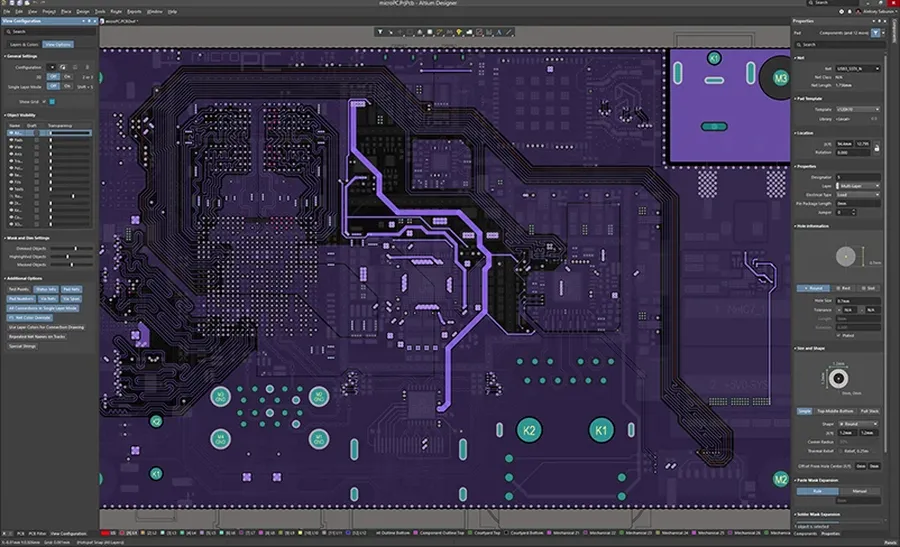
Altium Designer Interface
Altium Designer's interface is meticulously crafted to provide engineers with an efficient and intuitive environment for PCB design. It is structured around a central workspace, surrounded by various menus, toolbars, and panels, each designed to streamline different aspects of the design process. Mastery of this interface is pivotal for achieving optimal workflow efficiency and realizing complex designs.
Menus Located at the top of the application window, the menu bar provides access to a variety of commands organized logically, including file management, editing functions, and view options. Understanding these menu options is fundamental for interacting with Altium Designer effectively.
Toolbars Positioned below the menu bar, toolbars contain shortcuts to frequently used commands, categorized by function. These toolbars can be customized, allowing you to arrange tools that you use regularly for quick access. Customization leads to increased design speed and reduces time spent navigating menus.
Workspace The central area of the interface where design activities take place, the workspace displays schematics, PCB layouts, and other design documents. This area is highly configurable and can be adjusted to best suit your workflow, allowing for a focused design environment.
Panels Dockable windows that provide access to design information, library resources, project details, and more. These panels are typically located on the sides of the interface and can be opened, closed, and rearranged to suit your preferences. Effective use of panels significantly enhances design accessibility and information management.
Customization Customizing the interface allows engineers to optimize Altium Designer for specific tasks and workflows. This includes the placement of toolbars, panels, and the configuration of hotkeys. Tailoring the environment to individual preferences can substantially improve design efficiency.
Creating and Managing Projects in Altium Designer
Altium Designer Project
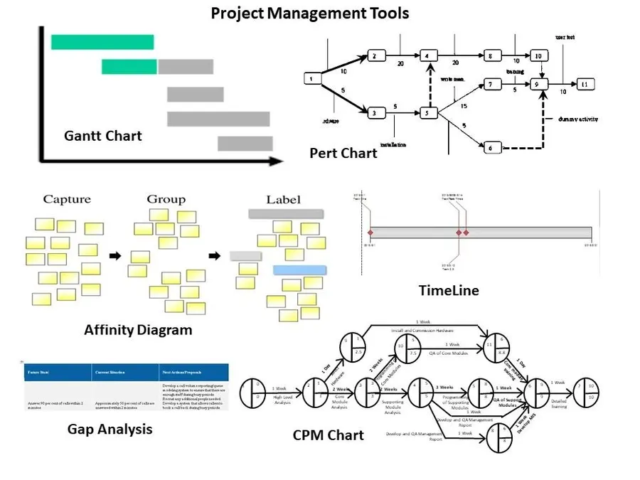
Efficient project creation and management are foundational to successful PCB design in Altium Designer. This section provides a comprehensive guide to establishing new projects, organizing design files, and ensuring a structured approach to your workflow, which is critical for maintaining design integrity and collaboration.
Project Creation Begin by selecting 'File' > 'New' > 'Project'. Choose the appropriate project type (e.g., PCB Project) and specify the location for your project files. Establish a clear naming convention for your projects to facilitate easy identification and retrieval.
File Organization Utilize a structured folder system within your project directory. Organize your design files into logical categories such as schematics, PCB layouts, component libraries, and output files. Consistent file organization prevents confusion and enhances team collaboration.
Project Options Configure project options to set up design rule checks, units, and other project-specific settings, according to your particular project requirements. Proper configuration ensures that all aspects of the design are aligned and will help to minimize errors during development.
Version Control Integrate version control systems (e.g., Git) to track changes, revert to previous states, and facilitate team collaboration. Version control is essential for managing complex projects and preventing data loss, and using version control helps to manage and track changes, and is an industry best practice.
Project Management Task
Best Practice
Purpose
Project Naming
Use a consistent naming convention (e.g., ProjectName_Version)
Facilitates easy identification and retrieval of projects
File Organization
Organize files into folders (Schematics, PCB Layouts, Libraries)
Prevents confusion and enhances collaboration
Design Rule Checks
Configure DR checks before beginning the design process
Ensures compliance with design standards and prevents manufacturing issues
Version Control
Utilize Git for version tracking and team collaboration
Enables efficient change management and minimizes data loss
Schematic Capture Basics
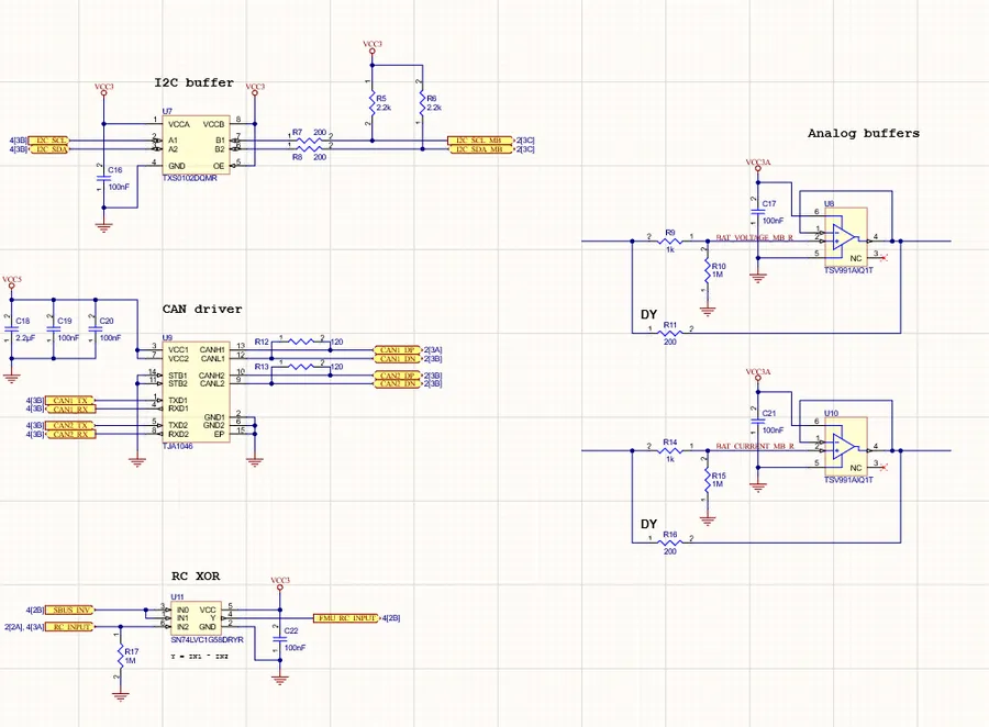
Schematic Diagram
Schematic capture forms the foundational stage of PCB design in Altium Designer, involving the graphical representation of electronic circuits. This process includes the strategic placement of components, the establishment of electrical connections through nets, and adherence to fundamental schematic design principles. Altium Designer's robust toolset facilitates an intuitive and efficient schematic creation process, ensuring design integrity.
Component Placement Strategic placement of electronic components from libraries onto the schematic sheet is a critical first step. Each component symbol represents an actual electronic part and must be placed logically for clear circuit representation.
Net Connections Establishing electrical connections between component pins using nets is how the schematic defines the flow of electricity. Altium Designer allows for both manual and automated net connection techniques, ensuring accuracy and efficiency.
Design Principles Adhering to essential design principles (such as avoiding crossovers and ensuring a clean and readable layout) ensures that the schematic accurately reflects the intended functionality of the electronic circuit. This is crucial for the later stages of PCB layout and for overall maintainability.
Schematic Element
Description
Function in Design
Components
Symbols representing electronic parts (resistors, capacitors, ICs etc.)
Building blocks of the circuit
Nets
Electrical connections between component pins
Define signal and power flow
Annotations
Labels, values, and other information linked to components and nets
Provide clarity and context
PCB Layout Design Techniques
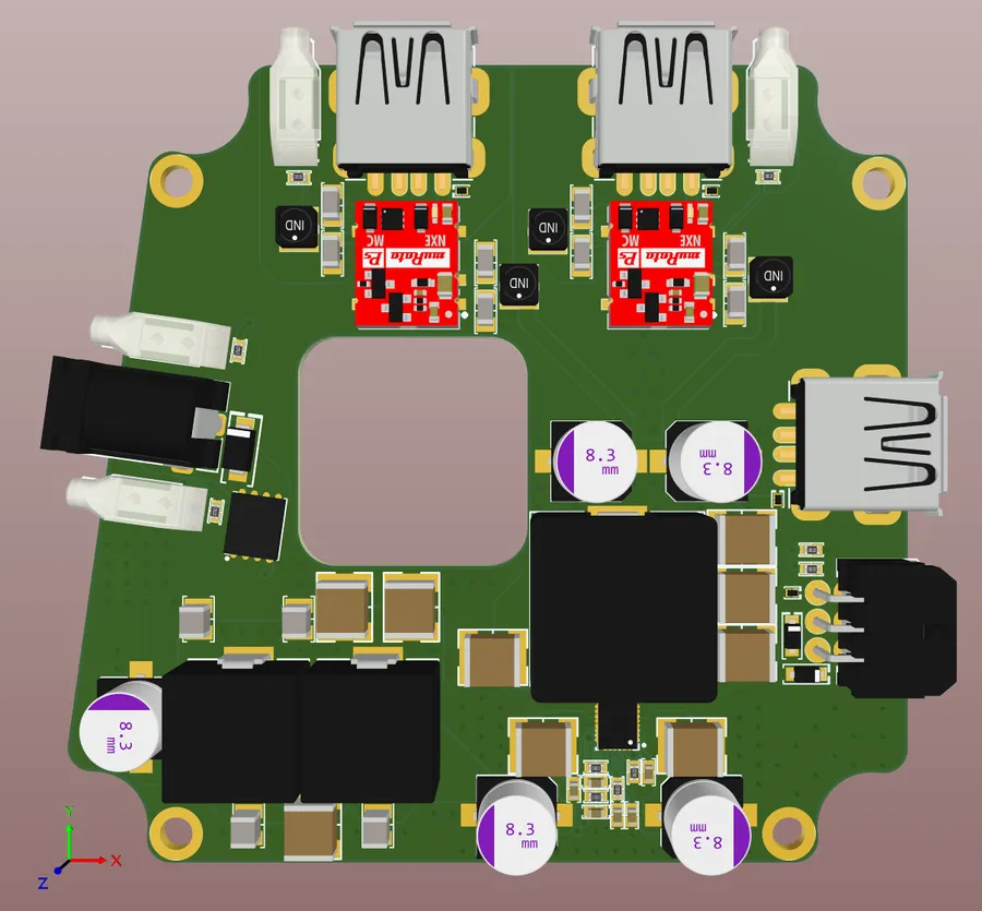
PCB Layout
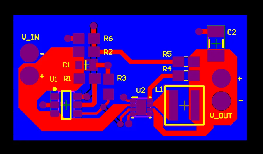
Effective PCB layout is critical for the functionality and reliability of electronic devices. Altium Designer provides a comprehensive suite of tools to master this process, encompassing footprint creation, component placement, routing strategies, and design rule checks, all essential for optimizing signal integrity and manufacturability.
Footprint Creation and Management Accurately define component footprints, crucial for physical board assembly. Altium's library system allows for both standard and custom footprint creation, including pad dimensions, solder mask definitions, and silkscreen markings. Proper footprint creation prevents assembly errors and ensures accurate component placement.
Component Placement Strategies Strategic component placement is crucial for efficient routing and thermal management. Considerations include component type, signal path requirements, and heat dissipation. Altium Designer offers tools for grouping, aligning, and distributing components to optimize placement within board constraints.
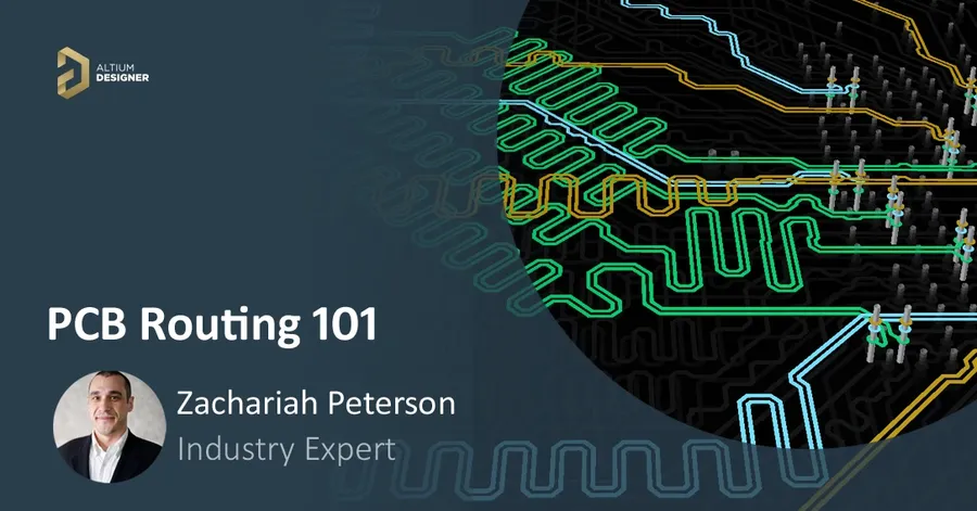
Routing Strategies Efficient routing ensures proper signal transmission and minimizes signal integrity issues. Altium provides both manual and auto routing tools, with various options including single-layer, multi-layer, and differential routing. Key techniques include minimizing trace length, controlling impedance, and avoiding sharp bends.
Design Rule Checks (DRC) DRC verifies design compliance with manufacturing specifications and electrical constraints. Altium's robust DRC system checks for violations such as trace widths, clearances, via locations, and layer stack-up. These checks are vital to ensure that the PCB can be fabricated and performs correctly in its intended application.
Technique
Description
Benefit
Differential Pair Routing
Routing two traces closely together with specific spacing.
Reduces electromagnetic interference (EMI) and noise for high-speed signals.
Impedance Matching
Controlling the trace width and layer stack to achieve a desired impedance.
Minimizes signal reflections and ensures signal integrity for high-frequency signals.
Via Management
Strategically placing vias to minimize signal distortion and maintain impedance.
Ensures reliable signal transition between layers.
Polygon Pours
Using copper pours to fill areas of the board.
Provides thermal management, reduces EMI, and creates ground planes.
By mastering these PCB layout techniques within Altium Designer, designers can achieve optimal board functionality, minimize production costs, and ensure product reliability. The software’s combination of design tools and verification checks offers a comprehensive environment for crafting high-quality PCB designs.
Component Libraries Management in Altium Designer
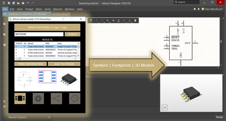
Component Library
Efficient management of component libraries is crucial for streamlined PCB design in Altium Designer. This section details the procedures for creating, modifying, and managing component libraries, emphasizing best practices for sourcing and integrating component data into your design projects within the Altium Designer environment, ensuring both accuracy and efficiency.
Creating Component Libraries Establish custom libraries by defining component symbols, footprints, and associated parameters. This ensures consistency and facilitates component reuse across different projects.
Modifying Components Learn how to update existing components, ensuring that modifications are reflected in all projects using the specific component, thus preventing inconsistencies.
Managing Components Implement strategies to organize component libraries, using categories and naming conventions, to ease searchability and facilitate quick access for design needs.
Sourcing Component Data Learn to integrate components from external sources and manage component data effectively to keep the library up-to-date, including utilizing manufacturer part numbers.
Integrating Components Learn how to incorporate custom components, along with vendor-supplied parts, ensuring that all associated data, including simulation models, are correctly set up within Altium Designer.
Library Aspect
Description
Best Practices
Component Creation
Defining symbols and footprints
Adhere to standards; use accurate dimensions
Component Modification
Adjusting existing component data
Document changes; test impact on existing designs
Library Management
Organizing and categorizing components
Use clear naming conventions; establish component categories
Data Sourcing
Importing component data from external sources
Use verified data sources; check for accuracy
Component Integration
Incorporating components into Altium Designer
Ensure accurate part matching; check for conflicts
Advanced Routing and Layer Management
PCB Routing
Efficient high-speed routing, impedance control, and effective management of multilayer PCBs are critical for optimal performance in electronic design. Altium Designer offers a suite of powerful features tailored to address these complex challenges, enabling engineers to push the boundaries of PCB design.
High-Speed Routing Techniques Altium Designer provides advanced routing tools to manage high-speed signals, including controlled impedance routing, differential pair routing, and length matching. These techniques are essential for maintaining signal integrity and minimizing signal degradation at high frequencies, as supported by best practices in high-speed digital design (e.g., Bogatin, Eric. *Signal Integrity Simplified*).
Impedance Control Maintaining consistent impedance along transmission lines is crucial for preventing signal reflections. Altium Designer allows designers to precisely calculate and control impedance using its layer stackup manager and interactive routing tools. This is aligned with electromagnetic theory principles as defined by industry standards such as IPC-2141.
Multilayer PCB Management Managing multilayer PCB designs can be challenging. Altium Designer streamlines this process with features like layer stackup visualization, layer pair selection, and via management. Proper layer assignment and via placement are crucial to avoid impedance discontinuities and signal integrity issues. As detailed in *Printed Circuit Board Design Using AutoCAD* by Chris Schroeder, good layer management practices reduce crosstalk and ensure reliable signal propagation.
Feature
Description
Benefit
Controlled Impedance Routing
Route traces with specified impedance values.
Ensures signal integrity and reduces reflections.
Differential Pair Routing
Route differential pairs with matched lengths and spacing.
Minimizes common-mode noise and ensures proper signal transmission.
Length Matching
Adjust trace lengths to match propagation delays.
Prevents timing skew and maintains signal synchronization.
Layer Stackup Manager
Define and visualize layer structure.
Manages the PCB structure and controls impedance.
Via Management
Control via placement and usage.
Minimizes signal impedance discontinuities.
Simulation and Analysis Tools
Altium Designer's integrated simulation and analysis tools are crucial for identifying and resolving potential design issues before manufacturing. These tools empower engineers to assess signal integrity, thermal performance, and other critical parameters, ensuring robust and reliable PCB designs.
These capabilities allow for iterative design improvements, reducing costly prototype revisions and time-to-market delays, while increasing the overall quality of the final product.
Signal Integrity Analysis Evaluates signal quality, reflections, crosstalk, and impedance mismatches. Ensures high-speed signals are transmitted with minimal degradation.
Thermal Analysis Simulates heat dissipation across the PCB. Identifies hot spots and potential overheating issues, facilitating thermal management design improvements.
Circuit Simulation (SPICE) Performs electrical simulations to verify the functionality of your circuit before moving into the physical design process. SPICE can analyze DC, AC, and transient behaviors.
Advanced analysis options Altium offers more advanced analysis capabilities, sometimes through third-party integrations, covering areas like power distribution network (PDN) analysis, electromagnetic interference (EMI) and EMC analysis, and more.
Analysis Type
Purpose
Benefits
Signal Integrity Analysis
Assess signal quality and identify potential issues such as reflections and crosstalk.
Ensures reliable high-speed signal transmission; minimizes signal degradation.
Thermal Analysis
Simulate thermal behavior to detect overheating; optimize heat dissipation.
Prevents thermal-related failures; improves system reliability; ensures proper operating temperature.
SPICE Simulation
Verify circuit functionality via DC, AC, and transient analysis.
Validates the electrical design and enables iterative improvements; avoids costly design mistakes during PCB layout.
Manufacturing Output and Documentation
Gerber Files
Altium Designer streamlines the transition from design to manufacturing by providing robust tools for generating essential output files and comprehensive documentation. This ensures that your PCB designs can be accurately produced and easily understood by manufacturers and other stakeholders.
Gerber File Generation Generate Gerber files, the industry-standard format for PCB manufacturing. Altium Designer offers precise control over layer selection, aperture settings, and file naming conventions.
Bill of Materials (BOM) Creation Automatically generate accurate BOMs, including component details, manufacturer part numbers, and quantities, essential for procurement and assembly processes.
NC Drill Files Produce NC Drill files containing precise drill hole locations and sizes, facilitating accurate board fabrication.
Pick and Place Files Create Pick and Place files with component placement coordinates and orientations, enabling efficient automated assembly.
Assembly Drawings Generate detailed assembly drawings that provide clear visual instructions for component placement, aiding manual assembly processes.
Schematic and PCB Documentation Produce high-quality PDF documentation of schematics and PCB layouts, enhancing project communication and review processes.
Customizable Output Options Tailor output settings to match specific manufacturer requirements or preferred formats, enabling seamless integration into diverse workflows.
Output File
Description
Purpose
Gerber Files
Industry standard format for PCB manufacturing data, containing layer information.
Fabrication of PCBs
Bill of Materials (BOM)
List of components with part numbers and quantities.
Component procurement and assembly
NC Drill Files
File containing drill hole location, size, and plating information.
Drilling of holes on PCB
Pick and Place Files
Component placement coordinates, rotation, and reference designators.
Automated component placement
Assembly Drawings
Visual guide for component placement, often with instructions.
Manual assembly assistance
PDF Documentation
Schematic diagrams, PCB layouts, and design information in a portable format.
Project communication and review
Frequently Asked Questions About Altium Designer
This section addresses common queries about Altium Designer, offering concise and authoritative answers to help users understand its capabilities, cost, classification, and learning curve. This information is crucial for potential and current users to make informed decisions and optimize their design workflows.
What are the primary applications of Altium Designer? Altium Designer is predominantly used for the design and development of printed circuit boards (PCBs). Its functionalities span from schematic capture and PCB layout to simulation and manufacturing output generation. It is employed across various industries including consumer electronics, aerospace, medical devices, and automotive, enabling engineers to design complex electronic systems.
How much does Altium Designer cost? The cost of Altium Designer varies based on the type of license (e.g., perpetual, subscription) and the included features. Pricing models are tailored for individuals, small teams, and large enterprises. Generally, it is considered a premium tool, and exact pricing can be obtained by contacting Altium directly or through authorized resellers. Educational licenses are available at reduced costs for students and academic institutions.
Is Altium Designer considered a CAD software? Yes, Altium Designer is categorized as a CAD (Computer-Aided Design) software, specifically within the ECAD (Electronic CAD) domain. It’s a powerful tool that facilitates the design of electronic circuits and boards, encompassing aspects such as schematic drafting, PCB layout, and design verification. As an ECAD tool, Altium is distinct from mechanical CAD (MCAD) software, which is used for designing mechanical parts and assemblies.
How long does it typically take to become proficient with Altium Designer? The learning curve for Altium Designer varies based on an individual’s prior experience with electronic design tools. Beginners may require several weeks to grasp the basics, while a deeper mastery of advanced features and techniques usually requires several months. Proficiency is gained through consistent practice, online tutorials, and potentially formal training courses. A strong foundation in electrical engineering concepts will accelerate the learning process.
Can Altium Designer handle complex multi-layer PCB designs? Yes, Altium Designer is well-equipped to handle complex multi-layer PCB designs. Its features include sophisticated layer management tools, advanced routing options, and impedance control capabilities. These enable users to design and manage very dense and complex boards with high signal integrity requirements. It supports both rigid and flex circuits, making it suitable for a wide range of applications.
Does Altium Designer offer simulation capabilities? Yes, Altium Designer integrates simulation tools that enable signal integrity and basic thermal analysis. This allows designers to simulate the behavior of their circuits before manufacturing, identifying and mitigating potential design issues. Integration with external simulation tools also possible further detailed simulation capabilities are needed.
Is there a community support available for Altium Designer users? Yes, Altium Designer has a large and active community, where users share their experience and solutions through various platforms including the Altium forum, third party community forums and other public discussion channels. This community support provides valuable resources for learning, troubleshooting, and staying updated on the software's latest features and best practices.
Altium Designer is an indispensable tool for modern PCB design, offering a comprehensive platform for engineers and designers. By mastering the techniques outlined in this guide, from schematic capture to manufacturing outputs, you'll be well-equipped to create cutting-edge electronic products. Whether you're a beginner or an experienced professional, Altium Designer's powerful features and flexibility will significantly enhance your PCB design workflow and improve your designs.