From the complex electronics in our smartphones to the simple circuits in our home appliances, printed circuit boards (PCBs) are the silent heroes of modern technology. PCB fabrication is the crucial process of transforming these electronic blueprints into the physical boards that power our world. This article delves into the detailed world of PCB fabrication, covering each step with clarity, while considering the necessary steps and options for your projects.
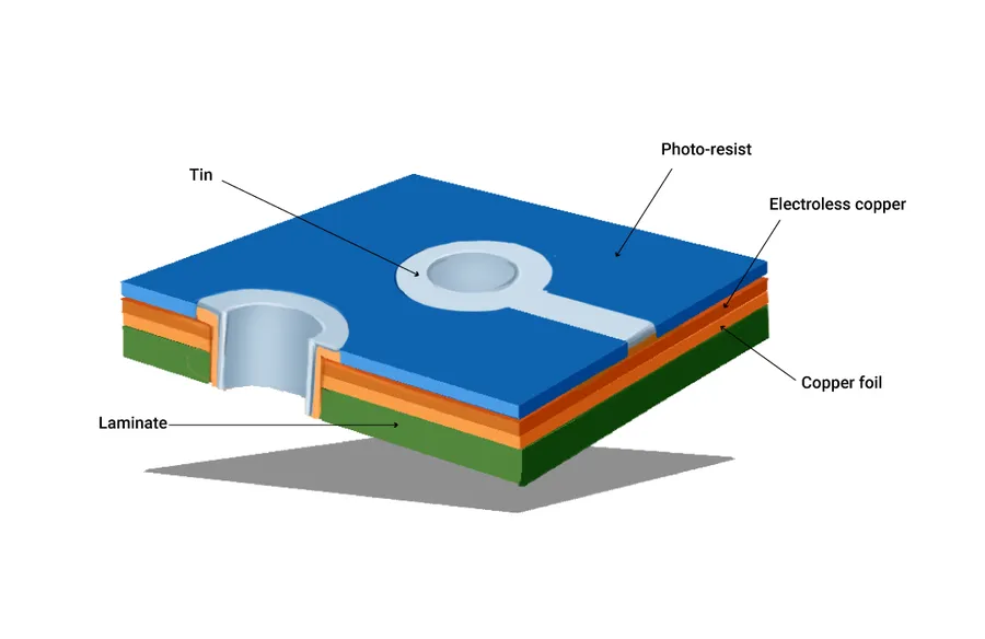
PCB fabrication is the multi-stage process of transforming a circuit board design into a physical printed circuit board (PCB), the foundational component for nearly all electronic devices. This involves sophisticated techniques such as layering, etching, drilling, and plating, employing various materials to construct a robust and functional circuit board, ready for component assembly.
The fabrication process can be broadly categorized into the following key stages:
Each stage is critical, requiring a high level of precision and quality control to ensure the final PCB meets the design specifications. The selection of materials and fabrication techniques will directly impact the board's performance, reliability, and cost.
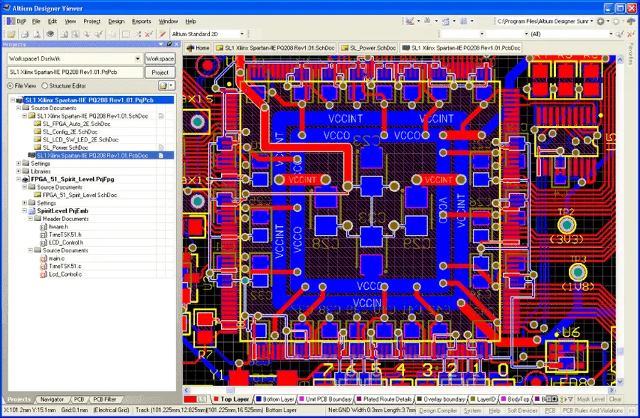
The initial design phase of a Printed Circuit Board (PCB) is crucial, as it dictates the functionality and manufacturability of the final product. This stage involves the use of specialized Computer-Aided Design (CAD) software to create precise PCB layouts. This process not only defines the physical placement of components, copper traces, and vias but also generates the necessary manufacturing files, specifically Gerber files, which are essential for the fabrication process.
| Design Consideration | Description |
|---|---|
| Signal Integrity | Ensuring high-quality signal transmission by controlling impedance and minimizing signal reflections through correct trace routing and layout. |
| Thermal Management | Optimizing component placement and adding heat sinks, thermal vias, or other thermal features to dissipate heat generated by components during operation. |
| Manufacturability | Designing the board considering the limitations of the fabrication process. Ensuring the design doesn't include excessively small features or require special manufacturing processes, which can increase costs and lead to difficulties. |
| Electromagnetic Compatibility (EMC) | Properly shielding components, managing ground plane layout, and implementing appropriate filtering to minimize electromagnetic interference to comply with regulatory standards. |
| Cost-Effectiveness | Using common components where possible to reduce the overall cost of the board and avoid unnecessary complexity and custom parts that can increase expense. |

The transition from a digital PCB design to a physical product begins with the preparation of production films. This critical step involves transferring the intricate circuit layout from CAD software onto physical films, which act as precise templates for the subsequent etching process. Accuracy in this stage is paramount, as any deviation can impact the final PCB's functionality.
This process utilizes photoplotters to generate highly accurate film representations of each layer of the PCB. These films, typically made of durable polyester, are treated with light-sensitive emulsion. The photoplotter exposes the film to light according to the Gerber files, resulting in a precise negative image of the copper circuitry. This image dictates where the copper traces will remain on the PCB, and where the copper will be removed during etching.
The materials required for this stage include the light-sensitive film, the photoplotter machine, and of course, the Gerber files, which are the industry standard file format for PCB designs. These files contain all the necessary data for each layer of the board. The quality of these materials and the precision of the equipment directly impact the fidelity of the final PCB.
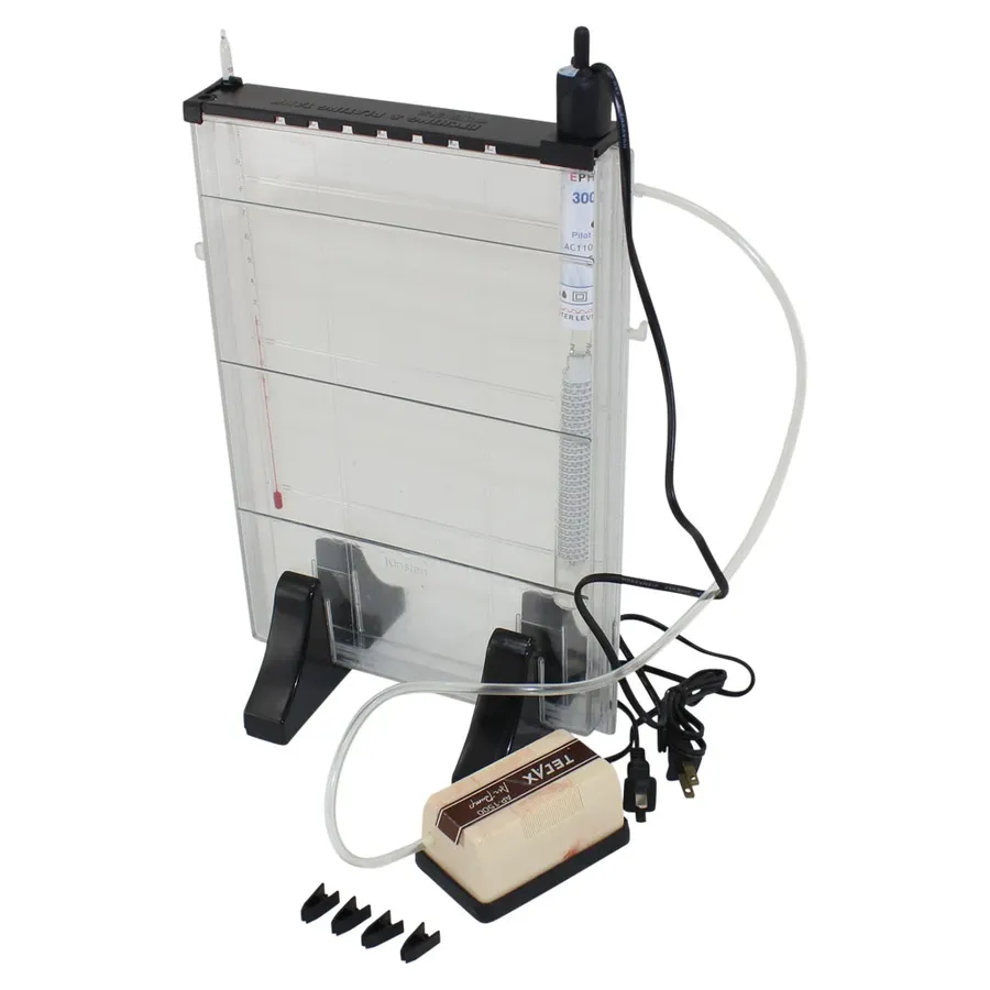
The layering and etching processes are fundamental to PCB fabrication, responsible for establishing the conductive pathways on the board. This stage involves creating the intricate copper traces that form the electrical circuitry. Precision and control during etching are critical to ensure the final board meets the required design specifications.
The process typically involves several key steps:
The etching process is highly sensitive to several parameters, including etchant concentration, temperature, and processing time. Variations in these parameters can lead to over-etching (resulting in thinner traces) or under-etching (resulting in incomplete removal of copper). Therefore, precise control is necessary for maintaining consistent trace widths and ensuring the electrical integrity of the PCB.
| Parameter | Impact on Etching Process | Importance |
|---|---|---|
| Etchant Concentration | Determines the rate at which copper is removed. | Optimal concentration ensures consistent etching and prevents over or under-etching. |
| Temperature | Influences the chemical reaction rate of the etchant. | Maintaining a consistent temperature is crucial for uniform etching across the board. |
| Processing Time | The duration of exposure to the etchant. | Precise control of time ensures the correct amount of copper is removed without damaging the traces. |
| Etchant Type | Different etchants have varying properties and etching rates. | Selecting the appropriate etchant for the specific copper thickness and desired trace quality is critical. |
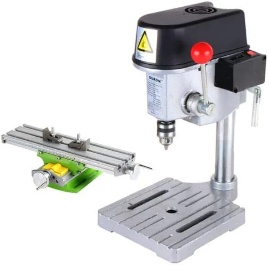
Precision drilling and subsequent plating are critical steps in PCB fabrication, ensuring electrical connectivity between different layers of the board through vias and through-holes. The accuracy of these processes directly impacts the final functionality and reliability of the printed circuit board.
Drilling creates the physical holes that allow for layer-to-layer connections. These holes can be vias (for internal layer connections) or through-holes (for connections across the entire board). After drilling, a plating process is employed to deposit a conductive material, typically copper, on the hole walls, creating an electrical path.
| Parameter | Description | Importance |
|---|---|---|
| Drill Diameter | Size of the drilled hole for vias and through-holes. | Critical for proper component lead insertion and electrical connectivity. Incorrect sizes can result in poor connections. |
| Drill Accuracy | Precision of the drill in hitting the designed locations. | Essential for ensuring that connections are made as designed and preventing short circuits. Poor accuracy may damage traces or pads. |
| Plating Thickness | Thickness of copper plating in the drilled holes. | Affects the electrical conductivity and mechanical strength of the plated through-hole or via. Insufficient thickness can lead to high resistance connections or open circuits. |
| Plating Uniformity | Consistency of copper plating on the walls of the drilled holes. | Ensures consistent electrical conductivity throughout the hole and good solderability. |
| Hole Wall Roughness | The surface finish of the interior hole wall after drilling. | Impacts plating adhesion and overall hole quality; too rough or inconsistent surface finish can result in a poor connection. |
Various drilling techniques, including mechanical drilling using precise drill bits and laser drilling for microvias, are employed based on the design requirements. Following drilling, a chemical deposition process prepares the hole walls for electroplating, after which copper is deposited to create the conductive paths. This whole process is tightly controlled to ensure the holes are of the correct size and that plating is complete and within the specifications required.
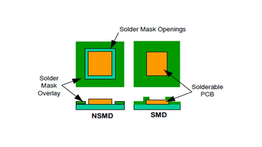
The application of soldermask and silkscreen is a critical step in PCB fabrication, serving to protect the board's circuitry and facilitate component placement and identification. These layers are not just cosmetic; they are essential for the long-term reliability and usability of the PCB.
Soldermask, a protective coating typically made of a polymer, shields the copper traces from oxidation, short circuits, and other environmental factors. Silkscreen, on the other hand, uses ink to print component designators, logos, and other essential information onto the board, aiding in assembly and debugging. Understanding the materials used and the application methods for these layers is key to producing a high-quality, long-lasting PCB.
| Feature | Soldermask | Silkscreen |
|---|---|---|
| Purpose | Protects copper traces from corrosion, shorts, and environmental damage. | Provides component designators, logos, and other identification markings. |
| Material | Typically a polymer-based material, available in various colors (e.g., green, red, blue). | Ink, often white, but other colors are available. |
| Application | Applied via screen printing or liquid photo imaging (LPI). | Applied via screen printing. |
| Thickness | Typically 10-30 μm. | Typically a thin layer, around 10-20 μm. |
| Key Function | Ensures electrical reliability and prevents unintended connections. | Facilitates assembly, testing, and repair; provides essential board information. |
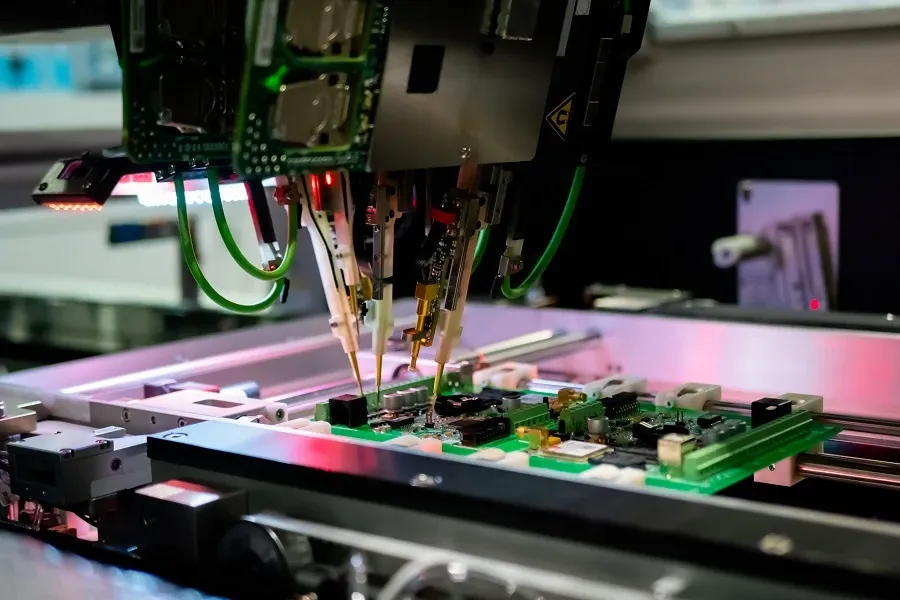
After the core fabrication processes, the printed circuit board undergoes final shaping (profiling) and rigorous testing to ensure its performance and reliability. These steps are crucial for validating the PCB's adherence to design specifications and its fitness for its intended application.
Profiling involves cutting the PCB from the larger fabrication panel to its final dimensions and shape using techniques like routing or laser cutting. Testing is a multi-faceted process designed to catch any defects introduced during fabrication and to verify the board’s electrical integrity.
| Process | Description | Purpose |
|---|---|---|
| Profiling | Physical cutting of the PCB to its specified dimensions and shape. | To create the final usable form factor of the PCB. |
| Visual Inspection | Examination of the PCB for any visible defects. | Identify flaws such as misaligned layers or damaged traces. |
| Electrical Testing | Applying electrical signals to test points and measure the board's response. | Confirming the electrical connectivity and integrity of the board. |
| Functional Testing | Simulating the operational environment of the PCB to test board functionality. | Verifying that the PCB performs as intended under operational conditions. |
| Quality Control | Systematic review of test data to confirm adherence to standards. | To ensure the PCB meets the required performance and manufacturing criteria. |
The testing phase might include a variety of methods, including continuity tests, impedance measurements, and functional tests where the board is powered and its performance is evaluated against the original design intent. Any boards that fail to meet these criteria are typically flagged for rework or scrapped, depending on the nature of the defect.
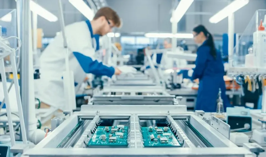
Selecting the appropriate PCB manufacturer is a critical step in ensuring the success of your electronic project. The ideal manufacturer will align with your specific needs concerning PCB complexity, production volume, budget, and deadlines. Evaluating manufacturers based on their capabilities, turnaround time, and cost is essential for achieving optimal results.
| Criteria | Description | Importance |
|---|---|---|
| Manufacturing Capabilities | The ability of the manufacturer to handle the complexity of your PCB design, including layer count, via types, trace width, material choice, and surface finishes. | Essential to ensure the manufacturer can produce PCBs according to your specifications and design requirements. |
| Turnaround Time | The duration required for the manufacturer to complete the fabrication process, from receiving the design files to shipping the finished PCBs. It is crucial for meeting project deadlines and timelines. | Critical for projects with strict time constraints, affecting product launch and overall project schedule. |
| Cost | The overall expense associated with PCB fabrication, including setup fees, unit costs, and any additional charges for specific requirements. It has a major impact on the overall budget of the project. | A significant consideration for staying within budget, particularly for large-scale or cost-sensitive projects. |
| Quality and Reliability | The manufacturer's adherence to quality standards, including material quality, dimensional accuracy, and testing procedures. Affects long-term performance, reliability and durability of the manufactured PCBs. | Crucial for ensuring that the PCBs meet performance expectations and function reliably in their intended environment. |
| Customer Support | The accessibility and responsiveness of the manufacturer's customer service and technical support. Having responsive and helpful customer support allows the project to progress smoothly. | Can greatly impact project efficiency and problem-solving during the fabrication process. |
| Minimum Order Quantities (MOQ) | The minimum number of PCBs that a manufacturer will produce per order, which can significantly impact project costs, especially for small-scale or prototype projects. Manufacturers with flexibility on MOQs are beneficial for low-volume runs. | Important for small projects and prototypes, affecting the practicality of working with a certain manufacturer |
This section addresses common questions regarding PCB fabrication, clarifying the distinctions between fabrication and assembly, and elucidating the meaning of PCB within the fabrication context. By answering these frequently asked questions, we aim to bridge knowledge gaps and provide a more complete understanding of the PCB fabrication process.
PCB fabrication is a complex yet vital process in the development of electronics. Understanding the various stages, from initial design to final testing, allows for a deeper appreciation of the technologies we use daily. By carefully considering each step and choosing the right fabrication partner, you can ensure the success of your PCB-based projects. The key to a successful PCB project lies in a strong understanding of the fabrication process. This process involves numerous critical steps, from initial design to the final product, each of which is crucial to the board's functionality and longevity.

