In our daily lives, we rely on a consistent and stable supply of electricity for all our electronic gadgets. But what if these voltage levels fluctuated wildly, leading to device malfunctions? This is where the often-overlooked Zener diode steps in, acting as a crucial voltage regulator. This specialized diode allows current to flow 'backwards' under specific conditions, offering unique capabilities in circuit design and ensuring stable operation. In this article, we'll explore this essential component and its myriad applications, bridging from simple circuits to complex systems.
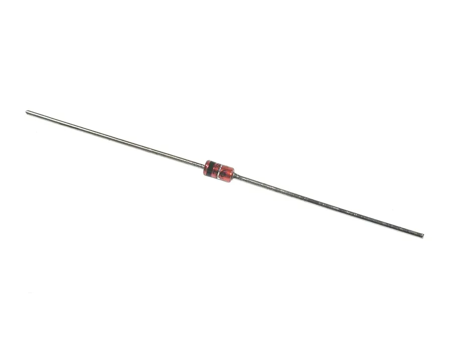
A Zener diode is a specialized type of semiconductor diode engineered to reliably conduct current in the reverse direction when a specific reverse voltage, known as the Zener voltage, is reached. This characteristic is in contrast to standard diodes, which are designed to block reverse current. The Zener diode's unique ability to operate in reverse bias makes it invaluable for voltage regulation and protection applications.
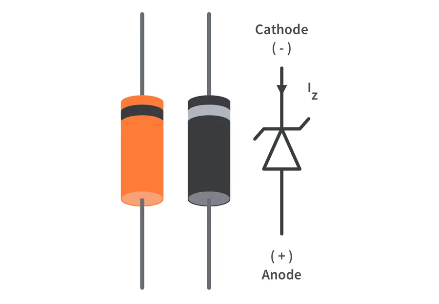
While both Zener diodes and regular diodes are semiconductor devices allowing current to flow primarily in one direction, their construction and behavior under reverse bias are fundamentally different. This distinction enables Zener diodes to perform voltage regulation and other specialized functions, whereas regular diodes do not.
| Feature | Regular Diode | Zener Diode |
|---|---|---|
| Primary Operating Bias | Forward Bias | Reverse Bias |
| Reverse Bias Behavior | Blocks Current (ideally) | Conducts at specific breakdown voltage |
| Doping Concentration | Moderate | Heavily Doped |
| Breakdown Voltage | High, often destructive | Specific, designed value |
| Primary Application | Rectification | Voltage Regulation |
The key difference lies in their doping levels and intended operation. Regular diodes are designed to block current flow in reverse bias until a high reverse voltage causes them to break down destructively. Zener diodes, however, are heavily doped to create a precise and non-destructive breakdown voltage, which allows them to conduct in reverse bias at this specific voltage, a property which is leveraged in voltage regulation and circuit protection.
The Zener effect is a quantum mechanical phenomenon that allows a Zener diode to conduct current in reverse bias when a specific voltage threshold, known as the Zener voltage, is reached. Unlike standard diodes which block reverse current until destroyed by excessive reverse voltage, Zener diodes are specifically designed to operate within this reverse bias breakdown region, offering a controlled and predictable way to handle reverse current.
This effect arises from the high electric field within the diode's depletion region. When a sufficient reverse voltage is applied, this strong electric field causes electrons to tunnel through the potential barrier of the depletion region from the valence band of the p-type material to the conduction band of the n-type material. This process, known as quantum tunneling, facilitates the flow of reverse current. The voltage at which this tunneling begins is relatively sharp and well defined, which makes the Zener diode useful for voltage regulation applications.
It's crucial to note that while the term 'Zener effect' is often used broadly to describe the reverse breakdown phenomenon in diodes, there are two related but distinct effects: the Zener effect and the avalanche effect. The Zener effect is dominant in diodes with lower breakdown voltages (typically below 5V) and is primarily due to quantum tunneling. The avalanche effect, dominant at higher breakdown voltages, involves impact ionization where high-energy electrons collide with atoms in the depletion region to generate additional free charge carriers. Often, both effects contribute to the breakdown behavior, and in the context of a Zener diode application, the combined effect is the functionality we utilize.
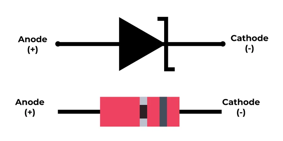
Understanding the schematic symbol for a Zener diode is crucial for interpreting circuit diagrams and designing electronic systems. Unlike a standard diode, the Zener diode's symbol clearly indicates its unique capability to operate in reverse bias. This section details the symbol and its proper representation within circuits, including an emphasis on polarity.
The Zener diode's schematic symbol is a variation of the standard diode symbol, featuring a bent cathode line, with two short lines that are slanting downward, that distinguishes it from standard diodes.
| Feature | Zener Diode Symbol | Standard Diode Symbol |
|---|---|---|
| Symbol | A triangle pointing to a vertical line with a bent cathode line (two short lines that are slanting downward) | A triangle pointing to a vertical line |
| Cathode | The bent line indicates the cathode terminal | The straight line indicates the cathode terminal |
| Polarity | Must be connected in reverse bias to utilize its zener effect; otherwise, conducts like a standard diode. | Primarily conducts current in the forward direction. |
In circuit diagrams, the Zener diode's polarity is crucial to its functionality. It's critical that the cathode, marked by the bent line, be connected to the more positive side of the circuit to utilize its voltage regulation capabilities in reverse bias. If connected in forward bias, it will conduct like a standard diode.
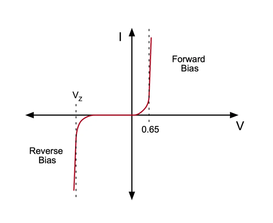
The voltage-current (V-I) characteristic curve of a Zener diode is pivotal for understanding its operation, revealing distinct behaviors in both forward and reverse bias conditions, with the reverse breakdown region being its key operational area. Unlike a standard diode, the Zener diode is specifically engineered to conduct current in reverse bias once the applied voltage reaches its characteristic Zener voltage (Vz).
| Parameter | Description | Symbol | Typical Value |
|---|---|---|---|
| Zener Voltage | The reverse voltage at which the diode breaks down and conducts current. This is the voltage the diode regulates at. | Vz | 2.4V to 200V |
| Test Current | The current at which the Zener voltage is measured. | Izt | Varies, depends on Zener power rating and voltage |
| Reverse Leakage Current | Current flowing in the reverse direction before breakdown. This current is very small but increase with temperature. | Ir | µA or nA |
| Maximum Power Dissipation | The maximum power that the diode can safely dissipate as heat. | Pmax | Varies, depends on the Zener physical size |
| Temperature Coefficient | Change in Zener voltage per degree Celsius change in temperature. | TC | mV/°C |
| Forward Voltage Drop | Forward voltage drop, similar to any diode | Vf | 0.6V to 1.0V |
Analyzing the Zener diode's V-I curve, several key parameters are apparent: * **Forward Bias:** In the forward direction, the Zener diode behaves like a standard diode, exhibiting a small forward voltage drop, typically around 0.7V for silicon devices. Current increases exponentially with the forward voltage. * **Reverse Bias (Below Vz):** When reverse biased and the voltage is less than the Zener voltage (Vz), a very small leakage current flows. This is similar to any standard diode behavior before its reverse breakdown. * **Reverse Bias (Breakdown Region):** Once the reverse voltage reaches the Zener voltage, the diode enters the breakdown region. In this region, the current increases rapidly with a minimal increase in voltage. The diode maintains a nearly constant voltage across it. This flat region makes the Zener diode ideal for voltage regulation. * **Zener Impedance:** In the breakdown region, the Zener diode has a dynamic impedance, meaning the change in voltage divided by the change in current. Ideally, this impedance is very low.
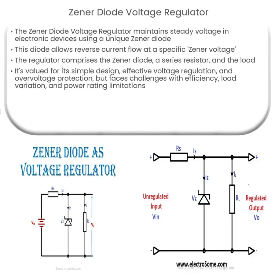
Zener diodes, when strategically incorporated into circuits, function effectively as voltage regulators by leveraging their unique reverse-bias breakdown characteristics to maintain a stable voltage output. This section explores this vital application, delving into circuit configurations and practical implementations.
The core principle of using a Zener diode for voltage regulation lies in its ability to maintain a nearly constant voltage across its terminals once its reverse breakdown voltage is reached, despite variations in input voltage or load current. This characteristic is crucial for providing a stable reference voltage in electronic circuits.
A typical Zener diode voltage regulator circuit consists of the Zener diode, a current-limiting resistor, and the load. The resistor is connected in series with the source, and the Zener diode is connected in parallel with the load. The resistor limits the current flow through the Zener diode, ensuring that it operates within its safe operating region and preventing damage due to excessive current. When the voltage across the zener diode reaches its breakdown voltage, it will begin to conduct current, which maintains a relatively constant voltage at that point
Consider a circuit with a 12V input, a 1kΩ resistor, and a 5.1V Zener diode. When the input voltage exceeds the Zener's breakdown voltage, the Zener diode shunts excess current to ground, maintaining a voltage of approximately 5.1V across the load. As long as the input voltage is higher than the Zener breakdown voltage, the output voltage remains relatively constant.
| Component | Function | Considerations |
|---|---|---|
| Zener Diode | Maintains a stable voltage at its breakdown voltage | Choose based on desired output voltage and power dissipation |
| Current-limiting Resistor | Limits the current flowing through the Zener diode | Select to prevent excessive current and diode damage |
| Load | Device requiring stable voltage | Should draw current within the regulator's capacity |
It is important to note that while the voltage across the Zener diode remains relatively constant, there can be some variation. The Zener diode's dynamic resistance will cause the output voltage to fluctuate slightly as the current flowing through it changes. Also, ensure that the power rating of the Zener diode is adequate for your current requirements. Zener diodes are not ideal voltage regulators, and they may not be the right choice for applications with very stringent precision requirements. They are nonetheless reliable and easy to implement.
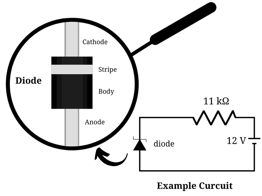
Zener diodes, with their unique ability to conduct in reverse bias when a specific voltage is reached, are essential components in various electronic circuits. This characteristic allows for their use in a range of applications, including voltage regulation, over-voltage protection, and signal clipping, providing reliable performance where stable voltage and protection are critical.
| Application | Description | Example Circuit |
|---|---|---|
| Voltage Regulation | Maintains a stable voltage across the load. | A Zener diode in parallel with a load, connected to a power source through a current-limiting resistor. |
| Over-voltage Protection | Protects components from voltage spikes. | A Zener diode in parallel with the component requiring protection. |
| Clipping Circuits | Limits the amplitude of a waveform. | Zener diodes connected to limit both positive and negative voltage peaks. |
| Reference Voltage Generation | Provides a stable voltage reference point in a circuit. | A Zener diode connected in series with a resistor to act as a stable voltage source. |
Selecting the correct Zener diode for a given application requires careful consideration of several key parameters to ensure optimal circuit performance and reliability. The primary factors are breakdown voltage, power dissipation, and tolerance, each affecting the diode's ability to function as intended.
| Parameter | Description | Importance |
|---|---|---|
| Breakdown Voltage (Vz) | The reverse voltage at which the Zener diode begins to conduct significantly and regulates voltage. | Crucial for voltage regulation applications, must match the desired output voltage. |
| Power Dissipation (Pd) | The maximum power the diode can safely dissipate as heat without being damaged. | Must be greater than the expected power dissipated in the circuit. Insufficient rating leads to failure. |
| Tolerance | The percentage deviation of the actual breakdown voltage from the nominal value. | Impacts the precision of the voltage regulation. Lower tolerance diodes are more accurate. |
| Temperature Coefficient | How the Zener voltage changes with temperature. | Important for applications exposed to temperature variations. A low temperature coefficient ensures stability. |
| Dynamic Impedance | The change in Zener voltage with respect to the change in reverse current. | Affects the quality of voltage regulation. Lower dynamic impedance results in better regulation. |
| Forward Voltage (Vf) | The forward voltage drop of the Zener diode when forward biased. | Relevant when the diode is not functioning in its breakdown region. |
| Maximum Reverse Current | Maximum allowable reverse current before damage. | Important for designing protective circuits. |
This section addresses common inquiries regarding Zener diodes, providing concise and practical answers to help clarify their behavior and applications.
In summary, the Zener diode is a versatile component crucial in many modern electronic circuits. Its unique ability to regulate voltage through reverse breakdown, a phenomenon linked to the Zener effect, sets it apart from conventional diodes. From voltage regulation to circuit protection, Zener diodes play an important role. As electronics continue to evolve, understanding and utilizing the properties of Zener diodes will be crucial in ensuring consistent and reliable performance.

