In today's tech-driven world, PCB (Printed Circuit Board) is the foundation of electronic devices. PCB fusion, the process of integrating design and manufacturing workflows, is streamlining electronics development. Using tools like Fusion 360, engineers and hobbyists alike can seamlessly move from concept to prototype, accelerating innovation. This guide will unravel the intricacies of PCB fusion, offering insights for both beginners and seasoned professionals to navigate the landscape of PCB design and manufacturing effectively.
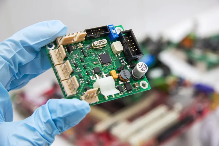
PCB fusion represents a paradigm shift in electronics design, converging traditionally separate stages of PCB development—design, simulation, and manufacturing—into a unified, iterative process. This integrated approach not only streamlines workflows but also significantly enhances the overall efficiency and precision of PCB production, resulting in fewer errors and faster time-to-market.
The traditional PCB development process often involves a fragmented approach where design, simulation, and manufacturing are handled using disparate tools and workflows. This separation can lead to several inefficiencies such as increased manual data transfers, higher chances of errors, communication breakdowns, and longer lead times. PCB fusion addresses these issues by combining these stages into a cohesive environment, allowing engineers to move seamlessly between design, analysis, and manufacturing preparation. The result is a more efficient, collaborative, and accurate product development cycle.
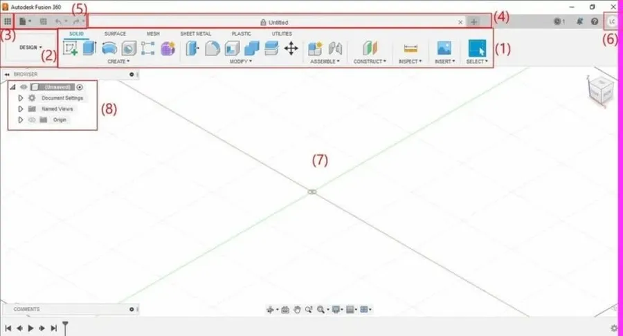
Autodesk Fusion 360 stands out as a powerful, cloud-based platform that seamlessly integrates various aspects of product development, including PCB design. This unified environment allows for a streamlined workflow from initial concept through detailed design and manufacturing preparation. Its key strength lies in its ability to bridge the gap between mechanical and electrical engineering, providing a holistic approach to product development.
| Feature | Description |
|---|---|
| Schematic Capture | Allows users to create electronic circuit diagrams, select components from libraries and define electrical connections. |
| PCB Layout | Provides tools for component placement, trace routing, layer management, and design rule checks. |
| 3D Visualization | Enables the creation and visualization of 3D models of the designed PCB, crucial for physical integration and interference checking. |
| Data Management | Centralized cloud-based storage and version control system for design collaboration and data tracking |
| Simulation capabilities | Basic simulation tools for checking thermal and stress performance |
| CAM Output | Tools to generate industry-standard Gerber files and other manufacturing data. |
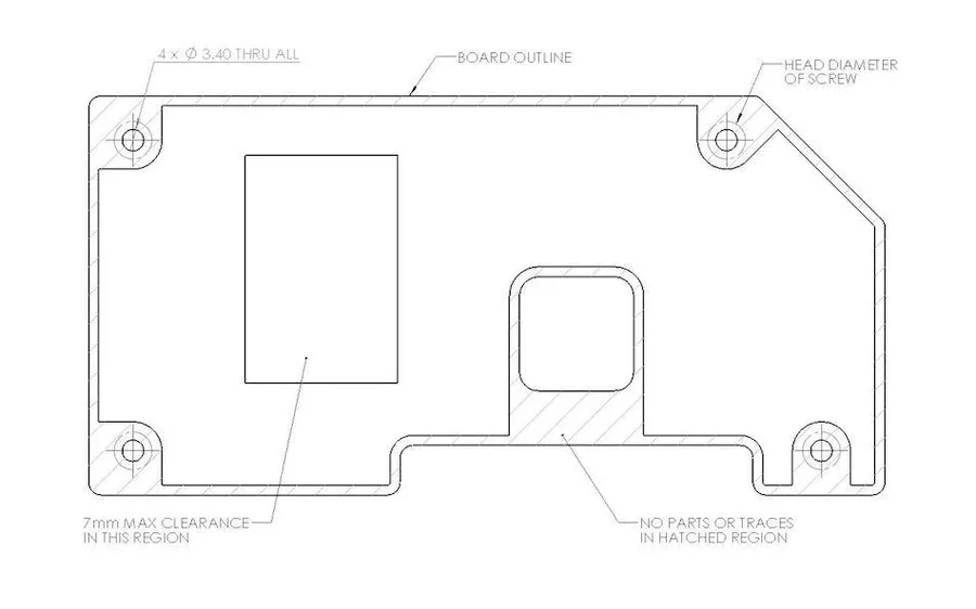
The foundation of any PCB design in Fusion 360 lies in creating an accurate board outline. This process involves sketching a precise 2D representation of your board's shape, which serves as the basis for component placement and routing. Fusion 360 enables the creation of both associative and independent 3D PCBs, each with its own advantages in design flexibility and project management.
| Feature | Associative PCBs | Independent PCBs |
|---|---|---|
| 2D Sketch Dependency | Linked to 2D sketch, changes propagate to 3D model | No link to 2D sketch |
| Modification Flexibility | 2D sketch changes automatically update 3D | 3D model must be modified directly |
| Workflow | Ideal for iterative design, quick changes | Better for very specific designs, avoids unintended changes |
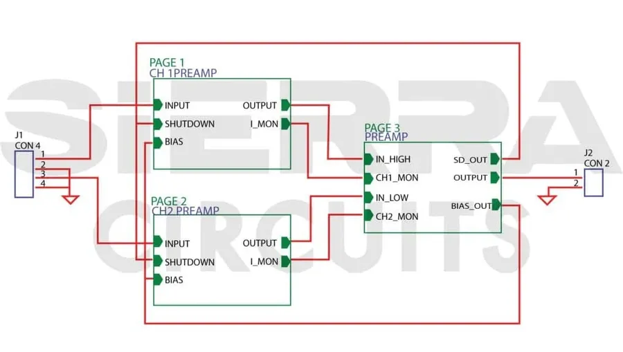
The schematic design phase in Fusion 360 is the crucial first step in transforming a conceptual electronic circuit into a tangible design. This stage involves representing the circuit using electronic symbols and connections, setting the stage for subsequent PCB layout and fabrication. This process prioritizes clarity and logical organization for easy understanding and modification.
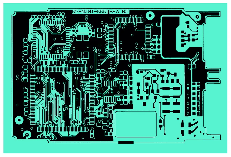
Efficient PCB layout and routing are critical steps in transforming a schematic design into a manufacturable printed circuit board. Fusion 360 offers a comprehensive environment for this process, allowing designers to manage component placement, define signal traces, and optimize board performance. This section will guide you through the key aspects of PCB layout and routing within Fusion 360.
| Aspect | Description | Best Practices |
|---|---|---|
| Component Placement | Strategic arrangement of components on the PCB. | Consider thermal properties, signal flow, and manufacturing requirements. |
| Trace Routing | Defining paths for electrical signals between components. | Minimize trace length, avoid sharp angles, and maintain proper spacing. |
| Layer Usage | Utilizing different layers for signals, power, and ground. | Optimize layer stacking for signal integrity and noise reduction. |
| Via Implementation | Employing vias to connect different layers of the PCB. | Use appropriate via sizes and placement to minimize signal impedance. |
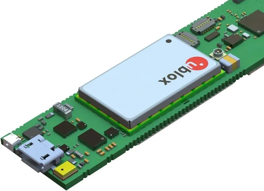
3D PCB modeling in Fusion 360 offers a crucial advantage by enabling designers to visualize their circuit boards in a three-dimensional environment. This capability goes beyond traditional 2D layouts, providing a realistic representation of the final product, and facilitating the identification of potential mechanical interferences, component clearance issues, and overall design flaws before manufacturing, saving time and resources by addressing problems early in the design cycle.
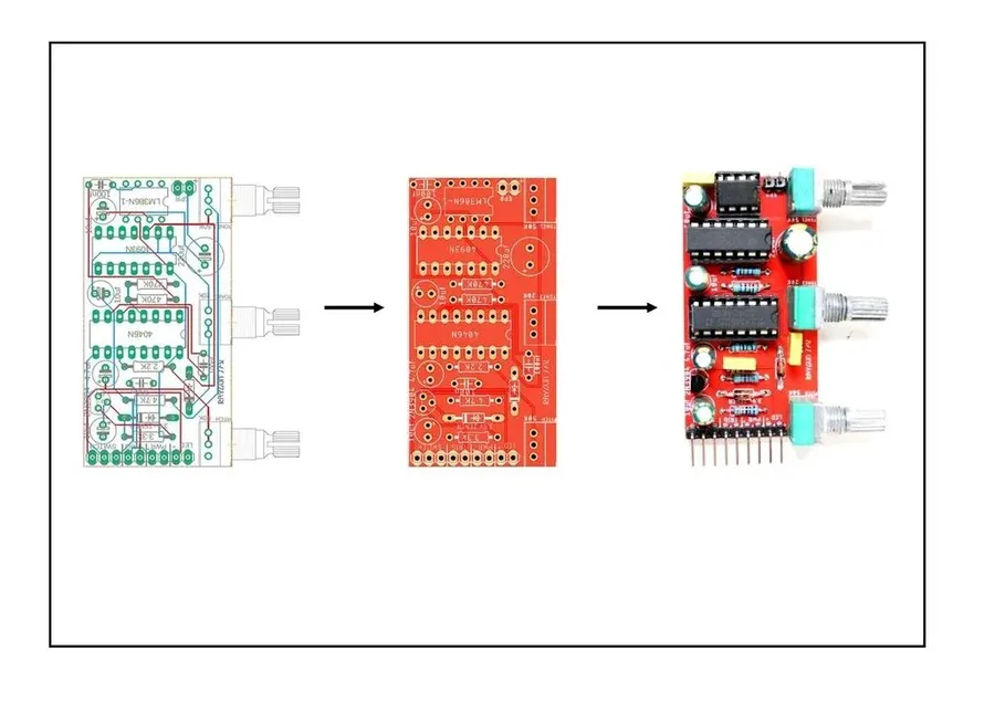
Preparing your PCB design for manufacturing involves generating the necessary files that fabrication houses use to create your physical board. Fusion 360 streamlines this process by allowing users to export industry-standard Gerber files and other manufacturing data, ensuring a smooth transition from design to production. This stage is crucial for achieving accurate and functional PCBs.
The primary output for PCB fabrication is the Gerber file set, which contains detailed information about each layer of your PCB design. This includes copper layers, solder mask, silkscreen, and drill data. Fusion 360 supports generating these files directly, simplifying the process.
Beyond Gerber files, manufacturing requirements can vary between different PCB service providers. Some might require additional files such as drill files in Excellon format or a Bill of Materials (BOM). Fusion 360 can generate these files, providing flexibility in choosing your manufacturing partner.
| File Type | Description | Purpose |
|---|---|---|
| Gerber Files | A set of files that define the copper layers, solder mask, silkscreen, etc. | Used for fabricating the physical PCB layers |
| Excellon Drill Files | Text-based files that specify the location and size of the drilled holes | Used for drilling the holes on the PCB |
| Bill of Materials (BOM) | A list of all components used in the PCB design, with manufacturer part numbers and quantities | Used for component procurement and assembly |
When selecting a PCB manufacturing service, several factors should be considered. These include the type of PCB (e.g., single-sided, double-sided, multi-layer), the required board thickness and materials, and special processing needs. Knowing your specific requirements will help you choose a manufacturer that meets your needs and budget.
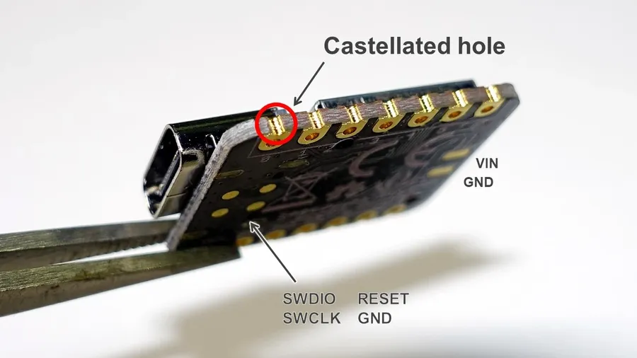
Selecting the right PCB manufacturer is crucial for turning your design into a physical product. This decision significantly impacts the final quality, cost, and lead time of your project. This section explores key considerations and introduces Seeed Studio as a viable option, while also touching on other potential manufacturers.
Choosing a manufacturer should go beyond just finding the cheapest option. A comprehensive evaluation involves assessing technical capabilities, production volume, turnaround time, and customer support, ensuring a smooth transition from design to a finished product.
| Factor | Description | Importance |
|---|---|---|
| Technical Capabilities | Includes precision, layer count, materials, minimum trace/space width, and advanced technologies. | Crucial for complex designs with tight tolerances. |
| Production Volume | Ranges from prototypes to mass production, affecting per-unit cost and scalability. | Select a vendor whose batch size capabilities match your project's needs |
| Turnaround Time | Refers to how quickly the boards can be produced, from design submission to finished product | Important for prototyping and time-sensitive projects. |
| Material Options | FR4 is common, but considerations include high-frequency laminates, flex substrates, etc. | Ensures that the material will meet application requirements |
| Cost | Balances manufacturing expense with quality, technology, and other needs. | Should align with your budget without compromising your project's needs. |
| Customer Support | Availability for technical questions and design for manufacturing (DFM) feedback | Valuable for both inexperienced and advanced users |
Seeed Studio is a popular choice, particularly for prototyping and small- to medium-volume production, due to their quick turnaround times, user-friendly online ordering platform, and support for various PCB specifications. However, there are many other PCB manufacturers that may be more appropriate, depending on the needs of your product.
This section addresses common questions regarding PCB fusion and the use of Fusion 360 for PCB design. We aim to provide clear, concise answers to help you navigate the process effectively.
PCB fusion, enabled by platforms like Fusion 360, represents a significant leap in electronic design and manufacturing. From schematic capture to 3D modeling and seamless integration with manufacturing, the process is now more accessible and efficient. Whether you're a seasoned professional or just starting out, the information discussed here should guide you in mastering the concepts of PCB fusion, driving your projects forward with speed and precision. By embracing the integrated design philosophy, you can unlock new possibilities in electronics innovation and bring your groundbreaking ideas to life effectively using PCB fusion.

