Printed Circuit Boards (PCBs) are the unsung heroes of modern technology, powering everything from smartphones to spacecraft. PCB design engineering is a specialized field that combines electrical engineering principles with artistic precision to create these complex and vital components. This article delves into the multifaceted world of PCB design engineering, providing a comprehensive guide for aspiring engineers and those curious about this dynamic discipline, covering essential skills, career paths, and the intricate design process involved in bringing electronic devices to life.
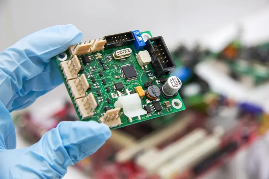
A robust grasp of fundamental electronics principles is the cornerstone of effective PCB design engineering. This involves a deep understanding of circuit theory, signal integrity, and power distribution, which dictates how well a PCB functions under various operational conditions. Neglecting these fundamentals can lead to performance issues, such as signal degradation, unstable power delivery, and ultimately, a non-functional electronic product.
The role of these fundamental concepts are: * **Circuit Theory:** Enables the engineer to understand how electrical current and voltage behave within the circuit. This encompasses understanding Ohm's law, Kirchhoff's laws, and various circuit analysis techniques. This knowledge forms the basis for how the components of the circuit will interact and is crucial for designing a functional circuit on the PCB. * **Signal Integrity:** Deals with maintaining the quality of electrical signals as they travel through the PCB. It focuses on minimizing signal distortion and ensuring that signals reach their destinations with minimal degradation. Factors such as trace impedance, reflections, and crosstalk are critical considerations in high-speed digital design. Signal integrity problems can lead to data corruption and unreliable operation. * **Power Distribution:** The method in which power is delivered to the components on the PCB. An effective design ensures that all components receive the required power with minimal fluctuations or noise. Improper power distribution can lead to unstable operation, component failure, and noise issues that can affect the entire system.
| Fundamental Principle | Description | Impact on PCB Design |
|---|---|---|
| Circuit Theory | Analysis of electrical circuits using Ohm's and Kirchhoff's laws. | Ensures correct voltage and current flow, proper component operation. |
| Signal Integrity | Maintaining signal quality during transmission. | Reduces signal distortion, reflections, and crosstalk for reliable operation. |
| Power Distribution | Efficient and stable supply of power to components. | Minimizes noise and fluctuations for stable and reliable component performance. |
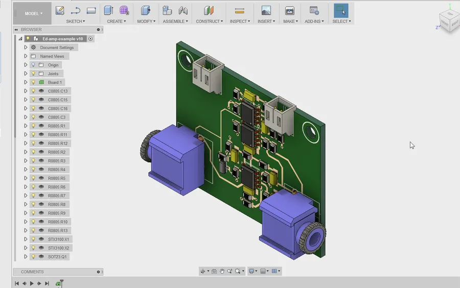
A successful PCB design engineer requires a robust combination of technical skills and problem-solving acumen. This role demands proficiency in several key areas, ranging from fundamental electronics knowledge to practical application of design software, and an understanding of manufacturing processes. Mastery in these areas allows engineers to create effective, reliable, and manufacturable PCB designs.
| Skill Category | Specific Skills | Importance |
|---|---|---|
| Technical Knowledge | Component knowledge, Circuit theory, Signal integrity, Power distribution | Essential for designing functional PCBs |
| Software Proficiency | EDA software usage, Schematic capture, PCB layout | Key for efficient design process |
| Fabrication Awareness | PCB manufacturing processes, material properties, DFM | Ensures designs are manufacturable |
| Analytical Skills | Problem-solving, debugging, optimization | Critical for overcoming design challenges |
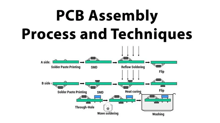
The creation of a printed circuit board (PCB) is a meticulous process that transforms an abstract electronic circuit design into a physical product. This process can be generally divided into several key stages, each requiring careful attention to detail to ensure the final product meets design specifications and functional requirements. These stages include schematic capture, component placement, trace routing, layer stack-up definition, and design validation, all of which contribute to the reliability and performance of the final PCB.
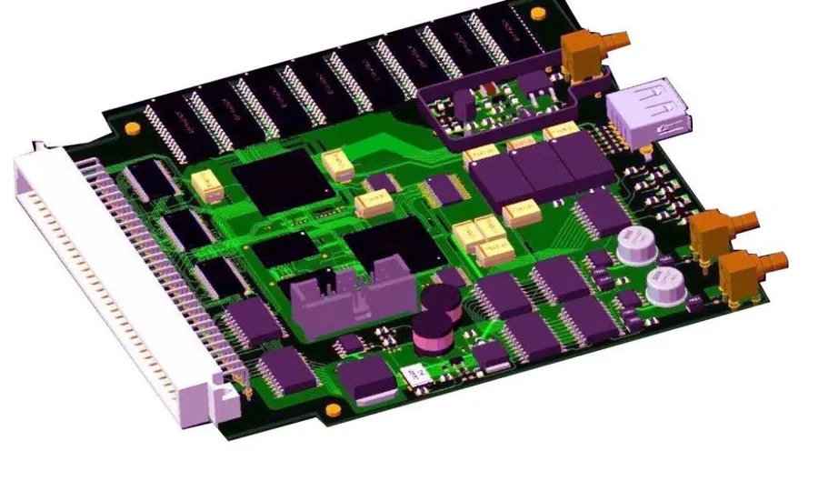
Selecting the appropriate PCB design software is a critical decision that profoundly affects a PCB engineer's efficiency and the overall quality of the final product. The market offers a range of Electronic Design Automation (EDA) tools, each with unique features, strengths, and limitations. This section delves into several leading EDA software options, including Altium Designer, Cadence Allegro, and KiCad, to guide you in choosing the tool that best aligns with your project requirements and technical proficiency.
| Software | Pros | Cons | Typical Use Cases | Pricing Model |
|---|---|---|---|---|
| Altium Designer | Comprehensive feature set, user-friendly interface, strong component library management, active community support. | Higher cost, can be resource-intensive, potential learning curve for beginners. | Complex, multi-layer boards, high-speed designs, professional environments. | Subscription-based |
| Cadence Allegro | Robust capabilities for advanced PCB design, excellent signal integrity analysis, suitable for large and complex projects. | Steeper learning curve, higher cost, more complex licensing. | High-density interconnect (HDI) designs, high-speed digital systems, aerospace and defense applications. | Perpetual License and Subscription Model |
| KiCad | Free and open-source, versatile, active community, good for small projects. | Less sophisticated feature set compared to commercial options, may require manual library management. | Hobbyist projects, educational purposes, small to medium-sized designs, prototyping. | Free and Open Source |
| EAGLE | User-friendly interface, good for small to medium projects, subscription available | Limited capabilities for complex designs, component library can be challenging. | Hobbyist projects, educational purposes, prototyping. | Subscription-based |
| PADS Professional | Complete schematic and layout tools, robust analysis and verification tools, strong integration with other design suites. | Higher cost and potential resource-intensive for smaller designs. | High-speed digital designs, analog circuits, and RF/microwave applications. | Perpetual License and Subscription Model |

The layer stack-up in a printed circuit board (PCB) is a critical design aspect that significantly influences signal integrity, impedance control, and electromagnetic compatibility (EMC). A well-planned stack-up optimizes performance by managing signal return paths, reducing crosstalk, and controlling impedance, while a poorly designed one can lead to signal degradation and increased noise.
The number of layers in a PCB stack-up can range from a simple two-layer board to complex multi-layer designs, depending on the specific application's requirements. Each layer has a specific purpose and contributes to the overall functionality of the PCB. Key considerations in designing a stack-up include layer material (dielectric constant), layer thickness, copper thickness, and the arrangement of power and ground planes.
| Layer Type | Function | Considerations |
|---|---|---|
| Signal Layer | Carries signal traces | Route traces to minimize impedance mismatches and crosstalk; careful placement of traces is critical for signal integrity. |
| Power Plane | Provides stable power distribution | Acts as a low impedance path for power delivery; essential for stable power and reduces noise. |
| Ground Plane | Serves as a return path and reduces noise | Creates an impedance reference; reduces electromagnetic interference and improves signal integrity. |
| Dielectric Layer | Insulates between layers | Determines impedance; Material dielectric constant effects performance. |
Specific configurations, such as the microstrip and stripline, also play a role. In a microstrip configuration, a signal trace is placed on the surface of the PCB with a ground plane below it. A stripline configuration, on the other hand, is where a signal trace is embedded between two ground or power planes, offering better EMC performance but higher fabrication costs.
Selecting the proper layer stack-up depends on the specific application needs, taking into account factors such as the signal frequency, the required impedance control, and the level of electromagnetic interference (EMI) expected. Careful analysis and simulation are recommended to ensure that the layer stack-up will provide optimal performance and compliance with design requirements.

PCB design engineering offers diverse career paths, from hands-on product development to specialized consulting roles. The field demands a blend of technical acumen and problem-solving skills, leading to various opportunities for professional growth and specialization. Advancement often requires continuous learning, mastery of new technologies and a keen understanding of industry trends.
| Career Path | Description | Required Skills | Advancement Opportunities |
|---|---|---|---|
| Product Development Engineer | Involved in the entire product lifecycle, from initial concept to final production. Designs and tests PCBs for specific products. | Strong understanding of electronic components, circuit theory, and PCB design software. Proficient in testing and validation methods. | Project lead, engineering manager, director of engineering |
| Hardware Engineer | Focuses on the overall hardware design of electronic systems, including PCB design and integration with other components. | Expertise in system-level design, integration, and testing. Familiarity with different hardware architectures and communication protocols. | Senior hardware engineer, technical lead, chief technology officer |
| Specialized PCB Consultant | Provides expert advice and solutions to clients, often focusing on complex designs or specific industry sectors. | Deep expertise in specialized areas like high-speed design, RF design, or thermal management. Excellent communication and problem-solving abilities. | Lead consultant, project manager, subject matter expert |
| Research and Development Engineer | Engages in research for next generation PCB design technologies and materials. | Strong background in materials science, advanced design techniques, and simulation tools. Innovative thinking is critical. | Research lead, principal investigator, academic positions |
| PCB Layout Designer | Specializes in the physical layout of PCBs based on schematics. Focus on efficient routing and manufacturability. | Proficiency in PCB layout software, understanding of design for manufacturing (DFM), and attention to detail. | Senior layout designer, layout team lead, design manager |
This section addresses common queries regarding PCB design engineering, offering clear and concise answers to help aspiring engineers understand the field. We aim to provide essential information about the role, career path, required qualifications, and how to successfully start a career in PCB design.
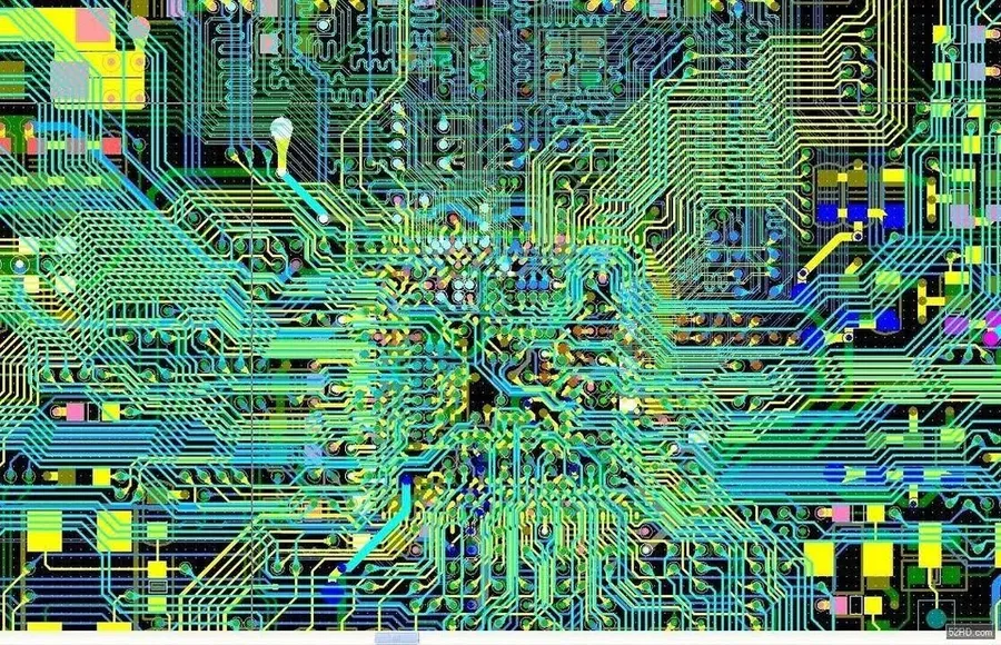
As PCB design engineering advances, specialization in niche areas becomes increasingly important. This section delves into advanced topics such as high-speed PCB design, thermal management, and RF PCB design, providing a deeper understanding of these critical aspects for experienced engineers looking to expand their expertise.
These advanced disciplines require in-depth knowledge of specific principles and methodologies beyond fundamental PCB design practices, focusing on performance optimization and signal integrity in increasingly complex designs. Further expertise in these areas positions engineers as highly specialized contributors within the industry.
| Topic | Description | Key Considerations |
|---|---|---|
| High-Speed PCB Design | Focuses on signal integrity and impedance control at high frequencies to ensure reliable data transmission. | Transmission line effects, impedance matching, crosstalk reduction, termination techniques. |
| Thermal Management in PCB Design | Addresses heat generation and dissipation to prevent component overheating and ensure reliable operation of electronic devices. | Heat sink design, thermal vias, airflow management, material selection. |
| RF PCB Design | Deals with designing printed circuit boards for radio frequency applications that need low signal loss, minimize interference, and achieve precise impedance control. | Antenna placement, impedance matching, shielding, substrate selection. |
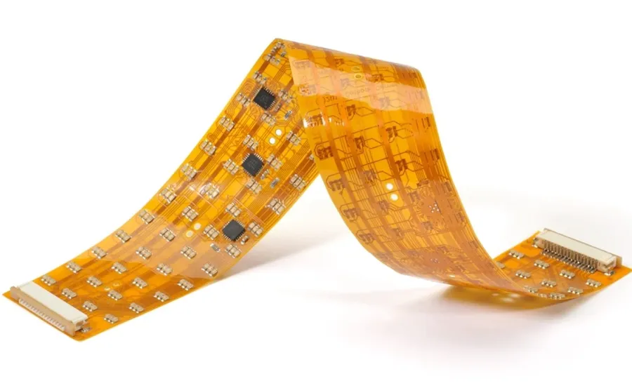
The field of PCB design engineering is undergoing a rapid transformation, driven by advancements in artificial intelligence (AI), automation, and material science. These innovations are not only streamlining the design process but also enabling the creation of more complex, efficient, and high-performance electronic systems. Adapting to these changes will be critical for PCB design engineers to remain competitive and innovative.
Below are key trends shaping the future of PCB Design Engineering:
PCB design engineering is at the forefront of technological advancement, enabling innovations across industries. A solid understanding of the fundamentals, paired with the right skills and continuous learning, will empower aspiring engineers to succeed in this dynamic and rewarding field. As technology continues to evolve, PCB design engineering will remain critical to the creation of cutting-edge devices. The future will require the development of more adaptable, sophisticated and innovative solutions to power next generation technologies and the design engineers will be right there on the front lines of innovation.

