In today's tech-driven world, digital integrated circuits (ICs) are the unsung heroes powering everything from our smartphones to supercomputers. This intricate field, known as digital integrated circuit design, involves crafting microscopic electronic circuits to perform logical operations. This article will guide you through the complex yet fascinating world of digital IC design, explaining its principles, processes, and practical applications, connecting it to the core of modern technology and innovation.
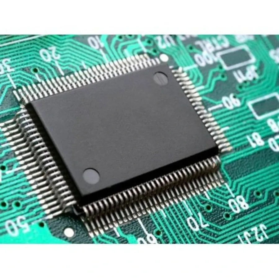
The foundation of digital integrated circuit (IC) design lies in the understanding of fundamental digital circuit building blocks. These include logic gates—such as AND, OR, NOT, NAND, NOR, and XOR—Boolean algebra, and number systems like binary and hexadecimal. These elements are crucial for implementing complex digital functionalities within integrated circuits.
| Concept | Description | Relevance to Digital IC Design |
|---|---|---|
| Logic Gates | Basic electronic components that perform logical operations on one or more inputs to produce a single output. | Form the fundamental building blocks for all digital circuits within ICs. |
| Boolean Algebra | A branch of algebra in which the values of variables are the truth values true and false, usually denoted 1 and 0, respectively. | Provides the mathematical framework for designing and analyzing digital logic. |
| Number Systems (Binary, Hexadecimal) | Methods for representing numerical values. Binary uses base-2 (0 and 1), while hexadecimal uses base-16 (0-9 and A-F). | Essential for representing and manipulating digital data within the IC. |
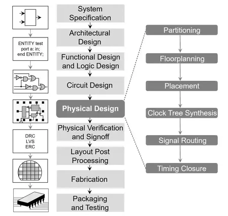
The digital integrated circuit (IC) design flow is a systematic and multi-stage process that transforms a high-level concept into a physical silicon chip. This flow ensures that the final fabricated IC meets the desired functional, performance, and reliability specifications. Each stage employs specialized tools and methodologies, requiring a deep understanding of both theoretical principles and practical implementation techniques.
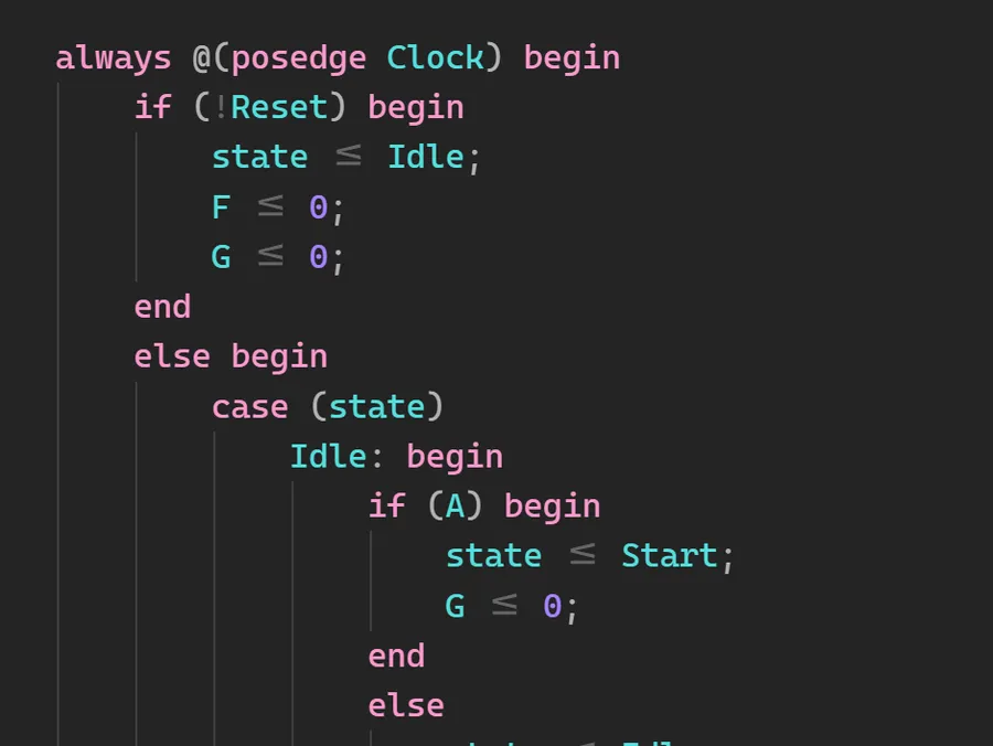
Hardware Description Languages (HDLs) are fundamental to modern digital integrated circuit design, providing a means to describe and model the behavior and structure of digital circuits at a high level of abstraction. Verilog and VHDL are the two dominant HDLs used in the industry, each with its own strengths and applications. Understanding these languages is crucial for any digital IC designer.
| Feature | Verilog | VHDL |
|---|---|---|
| Origin | Developed by Gateway Design Automation (now Cadence) in 1984. | Developed under the U.S. Department of Defense in 1980s. |
| Syntax | C-like, relatively concise and easier for software engineers to learn. | Ada-like, more verbose and strict, promoting structured design. |
| Abstraction Levels | Supports register-transfer level (RTL) and gate level descriptions well, suitable for design and verification. | Supports multiple abstraction levels from behavioral to gate-level, suitable for complex system design and simulation. |
| Data Types | Fewer built-in data types, more flexible but can lead to ambiguity. | Strongly typed with more explicit data types, enhancing code clarity and error detection. |
| Concurrency | Relies on procedural constructs (always blocks) to describe concurrent operations. | Explicitly supports concurrent operations through process statements, making concurrency representation more transparent. |
| Use Cases | Widely used in North America, particularly for ASIC design. | Commonly used in Europe and for complex, high-reliability designs including FPGA. |
| Learning Curve | Considered to have a gentler learning curve initially. | Steeper initial learning curve due to its verbosity and strong typing. |
| Industry Adoption | Highly adopted in industry and academia. | Strong adoption in industry, particularly in aerospace, defense and high-reliability applications. |
Both Verilog and VHDL are IEEE standards, ensuring their wide adoption and interoperability across various design tools. The choice between them often depends on project requirements, team expertise, and regional preference. Many design flows utilize both languages, leveraging their respective strengths at different stages of the design process.
Key considerations when working with HDLs include understanding their respective syntax, semantic nuances, and effective coding styles. High-quality HDL code is crucial for creating designs that are not only functionally correct but also synthesizable and performant. Efficient coding styles involve avoiding common pitfalls like race conditions, ensuring clear and modular designs, and employing the correct abstraction levels for the task at hand.
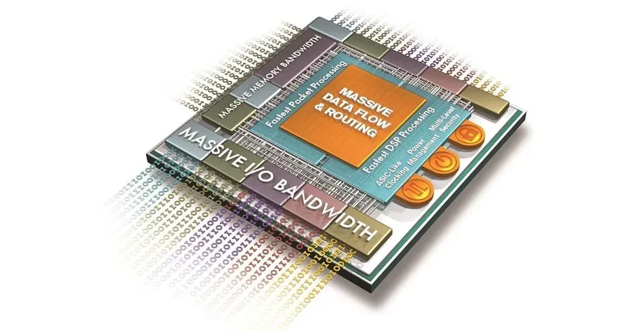
Digital integrated circuit (IC) design employs diverse methodologies to implement digital circuits, each with its unique advantages and trade-offs. This section delves into three prominent design styles: full custom, standard cell-based, and Field-Programmable Gate Array (FPGA) based design, exploring their characteristics, applications, and comparative aspects.
| Design Style | Description | Performance | Cost | Time to Market | Flexibility | Typical Applications |
|---|---|---|---|---|---|---|
| Full Custom | Layout and optimization of every transistor and interconnect. | Highest possible performance. Optimal area utilization | Highest cost for design and manufacturing. | Longest development time. | Maximum flexibility | High-performance ASICs, processors, memory controllers |
| Standard Cell | Utilizes pre-designed logic gates (standard cells) placed and routed automatically. | Good performance, slightly lower than full custom. | Moderate cost for design and manufacturing. | Moderate development time. | Moderate flexibility. | General-purpose logic, embedded systems, ASICs |
| FPGA | Implements logic using configurable logic blocks and programmable interconnections. | Moderate to lower performance. | Lowest initial cost, but can be expensive for high volume production | Fastest development time. | Highest flexibility | Prototyping, low-volume applications, adaptable hardware |
Choosing the right design style depends critically on project specific requirements and constraints. Full custom design, while offering unparalleled performance, demands significant resources and expertise. Standard cell design provides a balanced approach, suitable for many applications, while FPGA based design caters to prototyping and projects requiring flexibility and fast turnaround times.
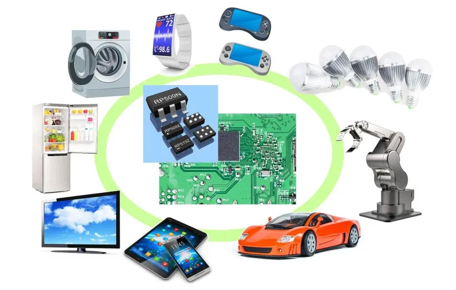
Digital integrated circuit (IC) design inherently involves a complex interplay between power consumption, performance, and the physical area occupied by the circuit. These three parameters are often interdependent, and optimizing for one can negatively impact the others. Achieving an optimal design requires a careful balance tailored to the specific application requirements.
| Parameter | Description | Unit | Impact |
|---|---|---|---|
| Power Consumption | The amount of electrical energy used by the circuit. | Watts (W) | Affects heat dissipation, battery life, and overall system reliability. Lower power is generally desired for portable and energy-efficient designs. |
| Performance | The speed at which the circuit performs its intended functions. | Hertz (Hz) for clock frequency; seconds for latency | Determined by clock frequency, propagation delays, and latency. Higher performance (higher clock frequency, lower latency) is desired but often comes at a power cost. |
| Area | The physical space occupied by the circuit on the silicon die. | Square millimeters (mm²) | Impacts cost, yield, and overall chip size. Smaller area is desirable for cost reduction and higher integration density. |
These key design parameters are tightly coupled, creating trade-offs that require careful consideration during the design process. For example, increasing the clock frequency to improve performance typically leads to higher power consumption. Similarly, reducing the area by using smaller transistors can result in higher leakage currents, which contribute to static power dissipation. Effective digital IC design involves employing various optimization techniques to navigate these constraints and achieve the best balance for the intended application.
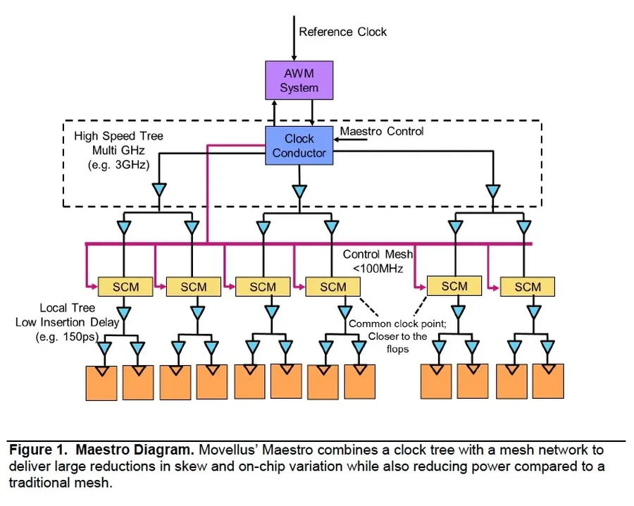
Advanced digital circuit design delves into sophisticated techniques to optimize performance, manage power, and ensure reliable operation. Key areas include clock distribution networks, pipelining, and various power management strategies, all crucial for high-speed and energy-efficient integrated circuits.
Clocking strategies are fundamental to synchronous digital circuits, with distribution networks needing careful design to minimize skew and jitter. Pipelining is a technique to increase the throughput of a circuit by introducing pipeline stages, effectively overlapping the execution of instructions. Finally, power management is paramount due to increased density and the need to limit power consumption and heat dissipation. These advanced techniques are essential for designing high-performance and energy-efficient integrated circuits.
| Technique | Description | Advantages | Challenges |
|---|---|---|---|
| Clock Distribution Networks | Delivers the clock signal to all parts of the chip with minimal skew and jitter. | Ensures synchronous operation of the digital circuits. | Difficult to design with low skew and jitter for large and complex chips. Susceptible to process variations. |
| Pipelining | Divides a processing task into multiple stages, allowing for concurrent execution. | Increases the overall throughput and clock frequency. | Increased latency. Can lead to increased area due to pipeline registers and more complex control logic. |
| Power Management | Techniques to reduce power consumption including dynamic frequency scaling, clock gating, and power gating. | Extends battery life, reduces heat dissipation and lowers cost. | Added complexity to the chip control. Can impact performance if not done well. Potential for performance penalty when switching between modes. |
Verification and testing are critical stages in the digital integrated circuit (IC) design process, ensuring that the final fabricated chip operates correctly and meets the predefined specifications. Verification aims to confirm the design's correctness before fabrication, while testing validates the fabricated chip's functionality against the specifications.
Both processes are essential for mitigating design flaws, reducing the likelihood of costly re-spins, and ensuring the delivery of reliable and high-quality integrated circuits. These steps occur at different design phases, employing diverse methodologies and tools.
| Aspect | Verification | Testing |
|---|---|---|
| Purpose | Ensure design correctness before fabrication | Validate fabricated chip functionality |
| Timing | Performed during design phases | Performed after chip fabrication |
| Methods | Simulation, Emulation, Formal Verification, Static Timing Analysis | Automated Test Equipment (ATE), Built-In Self-Test (BIST), Fault Modeling, Scan Testing |
| Goal | Detect design flaws and prevent costly re-spins | Ensure chip meets specifications and performs reliably |
This section addresses frequently asked questions regarding digital integrated circuit design, offering clear, concise answers to provide a deeper understanding of the field and its practical aspects. These questions range from career paths to software tools and emerging trends.
The field of digital integrated circuit (IC) design is rapidly evolving, driven by the ever-increasing demands for higher performance, lower power consumption, and greater integration density. Emerging trends like artificial intelligence (AI) integration, 3D ICs, and neuromorphic computing are poised to redefine the landscape of digital IC design, presenting both significant opportunities and formidable challenges.
Digital integrated circuit design is a complex field that sits at the heart of modern electronics. From fundamental logic gates to advanced power management techniques, this guide has explored the core concepts of digital IC design. By understanding its processes, tools, and considerations, aspiring and current engineers can contribute to the continuous evolution of technology and shape our digital future. The continuous advancements in this field, driven by innovation and the pursuit of performance and efficiency, make it a dynamic and essential area of study. With the growing demand for higher performing and more energy efficient devices, the future of digital integrated circuit design will remain an exciting frontier in engineering.

