In our increasingly interconnected world, printed circuit boards (PCBs) are the unsung heroes powering nearly all of our electronic devices. From the smartphones in our pockets to the sophisticated medical equipment in hospitals, these intricate boards rely on precision design enabled by PCB CAD software. Choosing the right PCB CAD tool is critical for hobbyists and professionals alike, impacting efficiency, design accuracy and overall product success. This article delves into the varied landscape of PCB CAD options, providing actionable insights to help you navigate this critical design space and master the creation process.
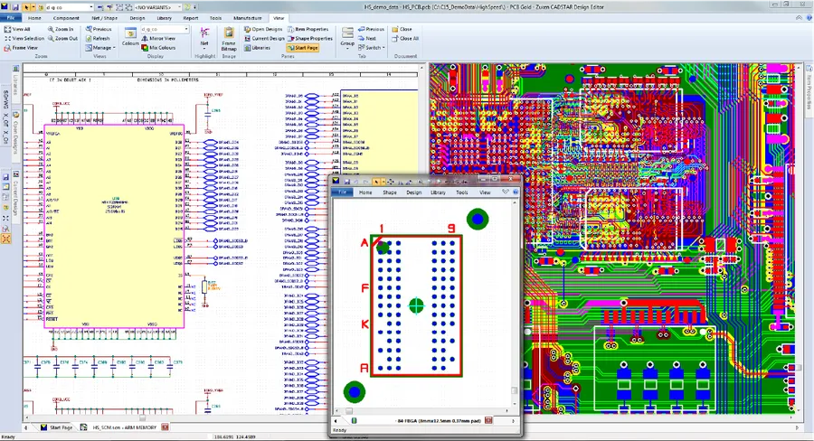
PCB CAD, or Printed Circuit Board Computer-Aided Design, is a specialized software domain focused on the design and layout of electronic circuits. Unlike general CAD software like AutoCAD, which deals with mechanical or architectural designs, PCB CAD is specifically tailored for creating the intricate patterns of conductive traces, vias, and component placements required for functional electronic circuit boards.
At its core, PCB CAD software empowers engineers and designers to translate abstract circuit schematics into physical layouts that can be manufactured. It provides a suite of tools that streamline the design process, significantly reducing manual effort and minimizing errors. This ensures the reliable, efficient, and accurate creation of complex electronic systems.
The advantages of using PCB CAD software are manifold. It allows for the rapid prototyping and modification of designs, which are vital in today's fast-paced electronics industry. These tools facilitate accurate component placement, ensure proper signal integrity through precise trace routing, and enable the generation of manufacturing files directly, optimizing the transition from design to production.
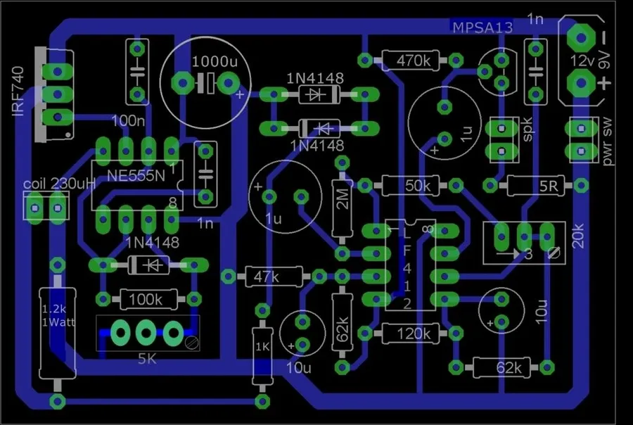
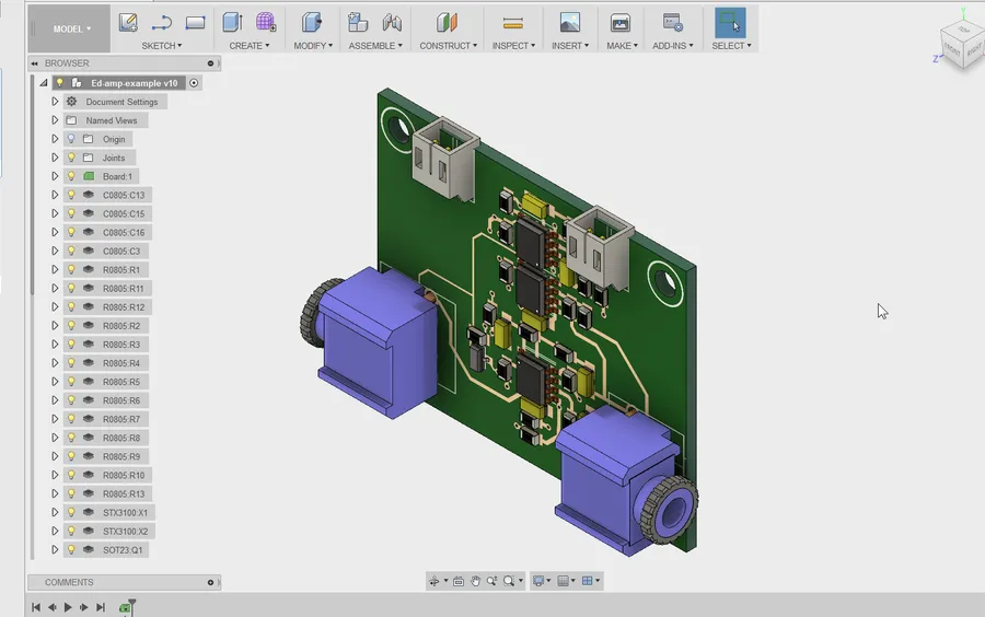
Selecting the appropriate PCB CAD software is crucial for efficient and accurate circuit board design. The ideal software should offer a robust set of features that streamline the design process, from schematic capture to final layout. Core functionalities include precise component placement, effective routing, comprehensive component libraries, simulation capabilities, and clear 3D visualization, which enhances the user's ability to assess the mechanical and spatial aspects of their designs. Ultimately, a balance of functionality and an accessible user interface is key to optimizing productivity and minimizing errors.
| Feature | Description | Importance |
|---|---|---|
| Schematic Capture | The ability to create and edit electronic circuit diagrams. It involves placing components, connecting them with wires, and assigning values and parameters. | Essential for defining the electrical connections and relationships between components. It provides the foundation for the PCB layout. |
| PCB Layout | Tools for designing the physical arrangement of components on the circuit board, including trace routing, pad placement, and copper pours. | Critical for translating the schematic into a manufacturable physical design. Effective layout ensures optimal electrical performance and signal integrity. |
| Routing Capabilities | Functionality for creating connections between components using copper traces. Includes features for automatic routing, manual routing, and via placement. | Efficient routing is key for signal integrity and minimizing electromagnetic interference. Good routing capabilities can significantly reduce design time and costs. |
| Component Libraries | A collection of pre-defined components with their physical and electrical characteristics. The library should be comprehensive and regularly updated. | Extensive and accurate libraries are essential for error-free designs and can save significant design time. |
| Simulation Tools | Tools that can simulate the behavior of the designed circuit, including signal analysis, thermal analysis, and electromagnetic compatibility. | Simulation capabilities help designers identify potential issues and optimize designs before manufacturing, thereby reducing the risk of costly errors and delays. |
| 3D Visualization | The ability to display the design in three dimensions. This helps designers verify mechanical fit and assess the spatial relationship between components. | 3D visualization is valuable for mechanical design checks and improves the understanding of the final assembled PCB. |
| User Interface and Ease of Learning | The overall user experience and the ease with which a new user can start to use the tool. | An intuitive user interface and well-structured workflow are important for minimizing the learning curve and ensuring an efficient design process. |
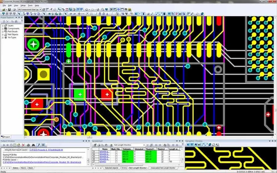
Selecting the appropriate PCB CAD software is crucial for efficient and effective circuit board design. This section provides a comparative analysis of leading software options, highlighting their strengths, weaknesses, pricing structures, and suitability for various user profiles. Our aim is to furnish a clear understanding of the landscape, enabling informed decisions tailored to specific project needs and budgetary constraints. We will delve into the functionalities of popular tools, ranging from industry-standard solutions to accessible open-source alternatives.
| Software | Strengths | Weaknesses | Pricing Model | Target User Group |
|---|---|---|---|---|
| Altium Designer | Industry-standard, comprehensive features, powerful routing capabilities, extensive component libraries. | High cost, steep learning curve for beginners. | Subscription-based | Professionals, large-scale projects, complex designs. |
| KiCad | Open-source, free, active community, robust feature set, cross-platform compatibility. | Less polished interface compared to commercial options, may require more user configuration. | Free | Hobbyists, students, small to medium-sized projects, open-source enthusiasts. |
| Autodesk EAGLE | Integrated with Fusion 360, good balance of features and price, user-friendly interface, available in free version. | Limited features in free version, can be less powerful than Altium for advanced designs. | Subscription-based, Free version available | Hobbyists, small to medium-sized businesses, maker community, educational users |
| EasyEDA | Free online platform, intuitive interface, suitable for beginners, easy collaboration, integrates with LCSC for component sourcing. | Limited features compared to desktop software, dependent on internet connectivity, less powerful for complex multilayer PCBs. | Free with optional paid features | Hobbyists, beginners, small projects, rapid prototyping, educators. |
| CircuitMaker | Free, community-driven, cloud-based, good balance of features, user friendly interface | Less features than Altium, potential for instability compared to desktop software | Free | Hobbyist, small scale professional projects. |
| DipTrace | User-friendly interface, moderate pricing, 3D visualization, good for mid-level complexity designs. | Fewer advanced features compared to Altium, less community support than KiCad. | Perpetual licenses available | Small to medium-sized projects, companies looking for moderate pricing and easy to use software |
| ExpressPCB | Extremely easy to learn, very simple interface, seamless integration with their fabrication services | Limited design capabilities, no Gerber output, tied to their fabrication services | Free to use with manufacturing | Very simple projects, single layer PCBs, users who require a very quick turnaround |
Selecting the appropriate PCB CAD software often involves a crucial decision: opting for a free or a paid solution. This choice is not solely determined by cost but also by the complexity of your projects, required functionalities, and the level of support needed. Understanding these differences is essential to ensure that the selected software aligns with your design requirements and budget.
| Feature | Free PCB CAD Software | Paid PCB CAD Software |
|---|---|---|
| Cost | No or minimal upfront cost. | Significant upfront or subscription costs. |
| Functionality | Basic features suitable for simple to moderately complex designs. May have limitations on design size or layers. | Advanced features for complex designs, including advanced routing, simulation, and analysis tools. Generally no limitations on design size or layers. |
| Component Libraries | May have limited, community-driven or less comprehensive component libraries. | Usually offer vast, professionally maintained component libraries. |
| Support | Community-based support forums and documentation. Often limited formal support. | Dedicated support channels, documentation, and tutorials. Faster response times. |
| Updates and Maintenance | May have less frequent or less rigorously tested updates. | Regular updates, bug fixes, and feature enhancements are provided. |
| Target Users | Hobbyists, students, and small-scale projects. | Professional engineers and enterprises handling complex projects. |
| Customization | Limited customization options. | Offers more extensive customization and scripting options. |
| Integration | May have limitations in integration with other design tools. | Often seamless integration with other design and manufacturing tools. |
The decision between free and paid PCB CAD software hinges on a balance between cost, functionality, and required support. Free options are excellent for learning, hobbyist projects, and simple designs, while paid options are geared towards complex, high-reliability designs that professional engineers often require. Carefully assess your needs to make the most appropriate choice.
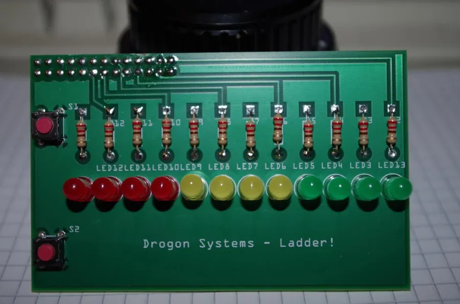
The selection of PCB CAD software is highly dependent on the user's specific needs, experience level, and project complexity. Different software packages cater to hobbyists, students, and professionals, each with distinct requirements in terms of features, learning curve, and cost. This section provides tailored recommendations to guide each user group towards the most suitable options.
For **hobbyists**, the primary focus is often on ease of use and cost-effectiveness. Many hobbyist projects are less complex, focusing on learning and experimentation rather than intricate design. Therefore, features such as intuitive interfaces, readily available tutorials, and free or low-cost options are crucial.
For **students**, educational institutions often require software that supports learning the fundamental principles of PCB design, but the budget can be limited. The software should offer features for schematic design, layout, and basic simulation to facilitate understanding the overall process.
For **professionals**, the emphasis shifts to software that can handle complex, high-density, and high-speed designs. These tools must offer advanced routing capabilities, strong simulation and analysis features, seamless integration with other design tools, and robust support. Time and efficiency in producing top-notch PCBs are key, and thus, cost becomes a secondary concern.
| User Group | Primary Needs | Recommended Software Options |
|---|---|---|
| Hobbyists | Ease of use, cost-effectiveness, basic features | KiCad, EasyEDA |
| Students | Educational focus, fundamental features, affordability | KiCad, Autodesk EAGLE (Student License) |
| Professionals | Advanced capabilities, high performance, industry standard | Altium Designer, Mentor Xpedition, Cadence Allegro |
This section addresses common questions about PCB CAD, providing clear and concise answers to help users understand its fundamental concepts and applications. This FAQ serves as a valuable resource for anyone seeking to deepen their knowledge of PCB CAD.
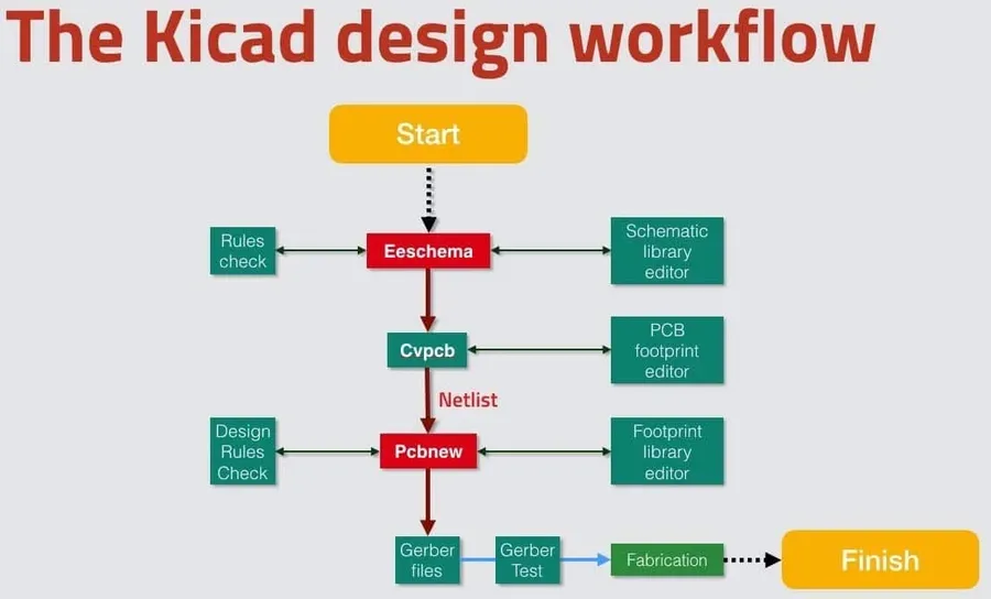
Efficient PCB design hinges on leveraging PCB CAD tools effectively. This section provides actionable tips and best practices to optimize your workflow, reduce errors, and improve overall design efficiency. Mastering these techniques will significantly enhance your PCB design process and final product quality.
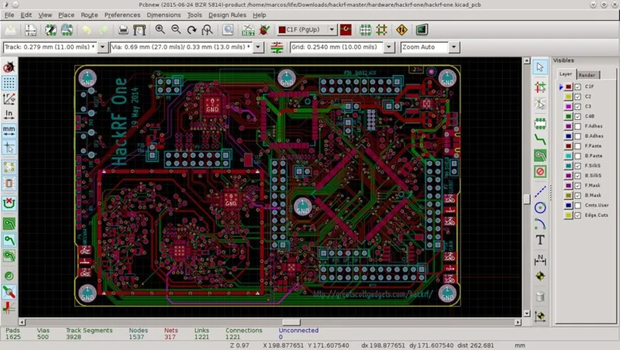
The landscape of PCB CAD technology is rapidly evolving, driven by advancements in artificial intelligence, cloud computing, and simulation capabilities. These trends are poised to transform how printed circuit boards are designed, manufactured, and tested, offering engineers unprecedented levels of efficiency and innovation.
The world of PCB CAD is constantly evolving, providing innovative solutions to meet the ever-growing complexity of electronic design. Whether you're a hobbyist taking your first steps or a seasoned professional pushing design boundaries, selecting the right PCB CAD software is crucial for success. Armed with this guide, you are now better equipped to navigate the numerous options and choose the tool that best aligns with your project needs. Remember, the ultimate goal of PCB CAD is to bring your electronic ideas to life efficiently and reliably. Embrace the technology and design with confidence using the best pcb cad tools available.

