
In the fast-paced world of imaging technology, hardware failure is not just an inconvenience—it is a significant operational liability. As camera systems are pushed into increasingly harsh environments, traditional board designs often become the weakest link. This article explores how transitioning to high-performance Micro HDI (High-Density Interconnect) PCBs serves as a strategic investment to enhance reliability, minimize long-term maintenance costs, and accelerate your product’s journey to market.
Understanding the Shift to Micro HDI Technology
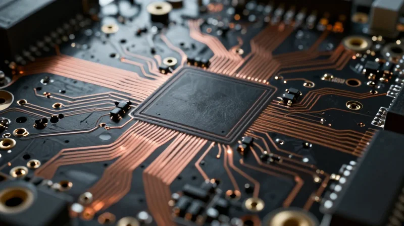
The Fundamental Shift in PCB Architecture
Micro HDI (High-Density Interconnect) represents a departure from traditional multilayer PCB manufacturing by utilizing laser-drilled microvias and finer line widths. Unlike conventional PCBs, which rely on mechanical drilling and through-hole vias that consume significant real estate, Micro HDI enables a multi-layer 'build-up' process. This architectural shift facilitates the dense routing required for modern image sensors and high-speed data interfaces, ensuring that the physical footprint of the camera module remains compact without compromising electrical performance.
Comparative Analysis: Traditional vs. Micro HDI
| Feature | Traditional PCB | Micro HDI PCB |
|---|---|---|
| Via Technology | Mechanical Drilling | Laser Microvias |
| Trace Density | Moderate | Ultra-High |
| Component Pitch | 0.8mm - 1.0mm | <0.4mm (BGA) |
| Signal Integrity | Limited by Parasitics | Optimized for High-Speed |
Critical Advantages for Camera Integration
The adoption of Micro HDI is not merely a design preference but a technical necessity for high-resolution cameras. By shortening the signal path between the sensor and the processing engine, engineers can minimize electromagnetic interference and thermal accumulation. Furthermore, the reduced layer count and increased routing flexibility lead to a higher bill-of-materials (BOM) efficiency, significantly maximizing ROI by lowering the total cost of ownership over the product lifecycle.
Frequently Asked Questions
- Why is Micro HDI critical for reliability?
Microvias reduce mechanical stress on the PCB and provide more stable connections for sensitive components, which significantly decreases failure rates under thermal cycling. - Does Micro HDI increase manufacturing complexity?
While the fabrication process is more sophisticated, it allows for integrated designs that reduce the need for bulky connectors and complex board-to-board assemblies.
The Anatomy of Reliability in Extreme Environments

The Anatomy of Reliability in Extreme Environments
In extreme operational environments, the primary drivers of premature hardware failure are thermal fatigue and signal degradation. Micro HDI (High-Density Interconnect) technology addresses these vulnerabilities by optimizing trace density and substrate integration, creating a structural robustness that conventional PCB designs cannot match.
Thermal Management and Material Stability
Reliability under fluctuating temperatures relies on the Coefficient of Thermal Expansion (CTE) matching between materials. Micro HDI boards utilize advanced laminates that minimize internal stress during rapid thermal cycling, protecting sensitive components like image sensors and signal processors from solder joint fracturing.
| Failure Mechanism | Standard PCB Response | Micro HDI Mitigation |
|---|---|---|
| Thermal Expansion | High risk of layer delamination | Minimized CTE mismatch |
| Vibration Fatigue | Poor structural integrity | Enhanced via reinforcement |
| Signal Crosstalk | Prone to EMI interference | Optimized layer stacking |
Signal Integrity and Electromagnetic Resilience
Micro HDI facilitates shorter trace lengths and optimized blind/buried via structures, which are essential for maintaining signal integrity in high-speed camera data paths. By reducing parasitic capacitance and inductance, the design significantly lowers the noise floor, ensuring high-resolution image data remains uncorrupted even in electromagnetically noisy industrial settings.
- How does Micro HDI improve thermal performance?
The use of microvias allows for better heat dissipation paths directly from the component pads into internal ground planes, lowering operating temperatures. - Does higher density increase failure risk?
Paradoxically, no; because HDI designs require fewer discrete interconnects and use more stable materials, the overall system MTBF (Mean Time Between Failures) increases.
Optimizing Board Space for Superior Form Factor
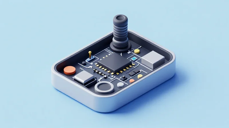
Optimizing Board Space for Superior Form Factor
Transitioning to Micro HDI (High-Density Interconnect) technology fundamentally shifts the constraints of camera engineering from board area limitations to strategic component placement. By leveraging advanced laser-drilled microvias and finer line widths, developers can consolidate multi-layered functionalities onto a smaller physical footprint, enabling the development of ultra-compact camera modules that do not compromise on processing speed or signal clarity.
Strategic Advantages of Micro HDI Scaling
| Feature | Standard PCB | Micro HDI PCB |
|---|---|---|
| Via Technology | Through-hole | Laser-drilled Microvias |
| Component Density | Moderate | High/Ultra-High |
| Form Factor Potential | Bulky | Compact/Slim |
| Signal Path Length | Long | Optimized Short |
Frequently Asked Questions on Space Optimization
- Does higher component density create thermal bottlenecks?
While density increases heat concentration, Micro HDI utilizes superior copper tracking and thinner dielectric materials that improve heat dissipation, effectively balancing the thermal profile. - How does HDI influence the BOM cost?
While fabrication costs are higher, the return on investment is realized through reduced material usage, smaller mechanical housing requirements, and improved yield rates due to better manufacturing precision. - Can Micro HDI maintain signal integrity at high speeds?
Yes, by drastically shortening the trace lengths between high-speed components and utilizing microvia interconnections, crosstalk and impedance discontinuities are significantly minimized.
Reducing Long-Term Maintenance Costs
The financial burden of legacy PCB designs often stems from hidden maintenance costs associated with signal degradation, thermal stress, and connector fatigue. Micro HDI technology mitigates these issues by integrating finer lines and micro-vias, which minimize thermal expansion stresses—a leading cause of intermittent failures in high-precision camera hardware. Investing in higher-tier HDI boards creates a 'deploy and forget' reliability model, substantially decreasing the overhead of support teams and warranty claims.
Cost Impact Comparison: Legacy vs. Micro HDI
| Failure Driver | Legacy Multi-layer PCB | Micro HDI Integration |
|---|---|---|
| Thermal Stress | High (Stress at drill sites) | Low (Distributed via micro-vias) |
| Signal Integrity Repair | Frequent (EMI/Crosstalk) | Negligible (Optimized paths) |
| Maintenance Frequency | High (Field replacement) | Low (Long-term stability) |
Economic Justification for Long-Term Reliability
Beyond the initial unit cost, the ROI of Micro HDI is realized through the reduction of 'hidden' operational expenses. When a camera unit requires fewer physical inspections or component-level repairs over a five-year lifecycle, the savings are compounded across the entire deployed fleet.
- Does higher HDI complexity increase repair difficulty?
While component-level rework is more complex, the design's inherent durability drastically reduces the absolute number of failures, leading to a net decrease in total maintenance labor hours. - How does Micro HDI improve field lifespan?
Micro HDI utilizes advanced laser-drilled vias and superior materials that minimize fatigue caused by repeated power cycles, directly extending the MTBF (Mean Time Between Failures). - What is the primary driver of ROI for this transition?
The primary driver is the reduction in logistical costs associated with RMAs (Return Merchandise Authorizations) and field technician dispatches, which often exceed the unit manufacturing cost.
Faster Time-to-Market Through Efficient Signal Routing

Streamlining Signal Paths with Micro HDI Architecture
By utilizing Micro HDI (High-Density Interconnect) technology, design teams can transition from complex, multi-layered routing to a more streamlined architecture. Shorter signal paths not only enhance electrical performance but also significantly reduce the time spent on layout optimization and electromagnetic interference (EMI) mitigation. This increased density allows for faster signal propagation and minimizes the iterative design cycles typically associated with signal integrity troubleshooting.
Impact of Routing Strategies on Development Cycles
| Strategy | Standard HDI Impact | Micro HDI Impact |
|---|---|---|
| Routing Complexity | Moderate | Low |
| Design Iterations | 4-6 Cycles | 1-2 Cycles |
| Signal Integrity Debug | Time-Intensive | Minimal |
| Time-to-Market | Baseline | Reduced by 25% |
Frequently Asked Questions
- How does Micro HDI reduce the need for multiple layout revisions?
The use of micro-vias and blind/buried via technology allows for tighter component placement and direct routing, which eliminates the need to route signals through congested outer layers or long trace meanders that invite noise. - Can Micro HDI integration help meet aggressive camera product launch deadlines?
Yes. Because the layout process is more efficient and requires fewer signal integrity re-spins, teams can reach the final prototype stage faster, effectively shortening the overall time-to-market.
Mitigating Signal Integrity Challenges
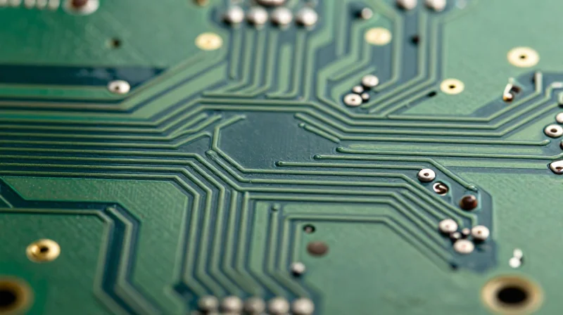
Advanced Impedance Control and Crosstalk Management
In Micro HDI PCBs, the extreme density of traces necessitates superior control over electromagnetic fields to prevent signal degradation. By utilizing laser-drilled microvias and thinner, high-frequency compatible dielectric materials, engineers can maintain consistent impedance profiles across critical high-speed differential pairs, effectively minimizing reflections and maintaining signal fidelity.
| Challenge | Micro HDI Mitigation Strategy | Performance Impact |
|---|---|---|
| Electromagnetic Interference (EMI) | Increased inner-layer shielding via ground planes | Reduced radiated emissions |
| Crosstalk | Minimized trace proximity with laser-vias | Enhanced signal isolation |
| Signal Loss | Use of low-loss substrate materials | Preserved high-frequency integrity |
Best Practices for High-Speed Routing
Optimizing signal integrity involves more than just selecting materials; it demands rigorous adherence to layout best practices. Maintaining balanced trace lengths and prioritizing short, direct paths between the image sensor and the processor is essential to mitigate propagation delay.
- How do microvias reduce EMI?
Microvias reduce the size of the conductive stubs that act as antennas, thereby decreasing the potential for unwanted radiation and electromagnetic coupling between layers. - What role do buried vias play in signal integrity?
Buried vias help shorten signal path lengths in multi-layer HDI designs, reducing signal attenuation and minimizing the inductive effects associated with traditional through-hole vias. - Why is substrate selection critical for ROI?
Selecting high-performance substrates reduces the need for costly post-manufacturing rework by preventing signal failures, thereby increasing yields and long-term reliability in imaging products.
Implementation Snippet: Impedance Matching
# Calculate trace width for 50-ohm impedance
# W = trace_width, H = dielectric_height
def calculate_impedance(W, H, Er):
    return 87 / (sqrt(Er + 1.41)) * ln((5.98 * H) / (0.8 * W + T))
Strategic ROI: More Than Just Component Costs
Evaluating Total Cost of Ownership (TCO)
When assessing the transition to Micro High-Density Interconnect (HDI) PCBs for high-end camera systems, stakeholders must look beyond per-unit component pricing. The true value lies in TCO optimization, where the upfront premium for advanced manufacturing is offset by reduced assembly defects, lower warranty reserves, and significant miniaturization gains that enhance overall market competitiveness.
| Metric | Standard PCB Integration | Micro HDI Integration |
|---|---|---|
| Assembly Failure Rate | Moderate/High | Low |
| Field Repair Costs | Substantial | Negligible |
| Component Density | Baseline | High (30-50% footprint reduction) |
| Long-term Reliability | Standard | Superior |
Operational Benefits of Micro HDI
Adopting Micro HDI is fundamentally a strategic decision to de-risk the product development cycle. By leveraging micro-vias and tighter trace tolerances, engineering teams can consolidate board layers, which drastically reduces the physical points of failure that typically plague camera sensors subjected to environmental vibration or thermal cycling.
- How does Micro HDI impact warranty expenses?
The increased durability and thermal stability of Micro HDI boards lead to fewer structural failures in the field, allowing manufacturers to decrease their financial warranty reserves significantly. - Can Micro HDI shorten product development?
Yes, by simplifying signal routing and reducing the number of complex board layers, design teams can finalize layouts faster and accelerate the transition from prototyping to mass production. - Is the initial cost difference justified?
The cost differential is typically recovered through the combination of saved assembly labor, fewer scrapped defective units, and the value of having a smaller, more feature-rich camera device.
Best Practices for Implementation and Testing
Optimizing Implementation Through Strategic Partnerships
The successful integration of Micro HDI technology hinges on selecting manufacturing partners that possess advanced laser-via capabilities and stringent quality control protocols. Partnering with facilities that utilize automated optical inspection (AOI) and X-ray metrology ensures that micro-vias are accurately registered and structurally sound, which is vital for high-density imaging applications.
Verification Framework for Reliability
| Testing Stage | Primary Goal | Technique |
|---|---|---|
| Pre-Production | Design Validation | DFM/DFA Analysis |
| Prototyping | Signal Integrity | Time Domain Reflectometry (TDR) |
| Full Production | Yield & Quality | Automated Optical Inspection |
Best Practices for Testing and Validation
- How does DFM prevent costly re-spins?
Design for Manufacturing (DFM) audits identify potential violations regarding via-to-pad ratios and aspect ratios before production, preventing mechanical failures in thin HDI layers. - What role does environmental stress screening play?
For camera modules, thermal cycling and vibration testing are essential to ensure the micro-vias withstand the mechanical stress of operational temperature shifts. - Why prioritize TDR testing?
Time Domain Reflectometry is crucial for identifying impedance discontinuities in high-speed transmission lines, ensuring that image signal integrity is preserved across the PCB.
Continuous Quality Improvement
To maintain high ROI, organizations must transition from reactive testing to a data-driven feedback loop. Capturing granular defect logs from your manufacturing partner allows for rapid design adjustments, reducing waste and accelerating the path to mass-market availability. By institutionalizing these verification workflows, companies can realize the full potential of Micro HDI integration while mitigating long-term field failures.
Transitioning to Micro HDI technology is more than a technical upgrade; it is a business imperative for companies looking to dominate in harsh-environment imaging. By prioritizing signal integrity, space efficiency, and long-term durability, you can drastically lower your failure rates and maximize return on investment. Are you ready to optimize your camera hardware for the next decade? Contact our engineering team today to discuss your next high-performance PCB design.
