
In the race to pack more optical power into smaller footprints, the PCB design has become the primary constraint. Designing for high-density interconnects (HDI) in cameras requires more than just standard layout practices; it demands rigorous DFM adherence to ensure that the microscopic interconnects can withstand the vibration, thermal cycling, and physical shock inherent in field-ready ruggedized electronics.
The Evolution of HDI in Small-Form-Factor Optics
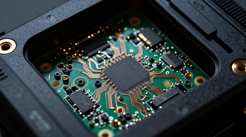
As the demand for high-resolution, high-frame-rate action cinematography grows, the circuit board real estate in ruggedized cameras has shrunk even as component density has intensified. The transition toward micro-HDI architectures is no longer optional; it is a fundamental requirement for maintaining signal integrity and power delivery for next-generation image sensors and ultra-compact ISP chipsets.
Drivers of HDI Miniaturization
The shift toward advanced HDI processes is primarily driven by the need to manage increased data throughput from high-megabit sensors. This requires tighter pad pitches and smaller trace widths, often pushing manufacturing into the realm of Advanced HDI (Any-Layer) technologies. Ruggedized environments further compound these challenges by necessitating mechanical resilience against vibration and thermal cycling.
| Feature | Standard HDI | Advanced Micro-HDI |
|---|---|---|
| Via Structure | Blind/Buried | Any-Layer (ELIC) |
| Min Line/Space | 50/50 micron | 25/25 micron or less |
| Aspect Ratio | 1:1 | 1:0.75 |
| Reliability | High | Enhanced (Shock/Thermal) |
Critical Technical FAQ
- Why is Any-Layer HDI (ELIC) critical for action cameras?
Any-Layer Interconnect (ELIC) allows for flexible via placement anywhere on the board, significantly reducing PCB layer counts and enabling the compact vertical stacking required for high-density camera modules. - How do DFM rules change for ruggedized applications?
Advanced DFM rules focus on enhancing structural rigidity by optimizing copper balance, enforcing strict pad-to-hole registration tolerances, and utilizing specialized solder mask coatings to withstand harsh environmental impacts. - Does micro-via miniaturization impact manufacturing yield?
Yes, laser drilling smaller holes increases aspect ratio challenges. Manufacturers must implement precise pulse control and desmear processes to ensure reliable, void-free copper plating in microscopic vias.
Material Selection: Balancing Impedance and Mechanical Integrity
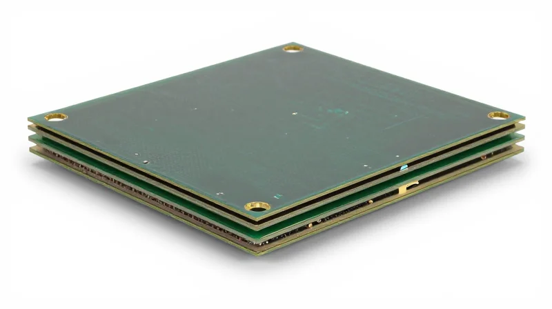
For action cameras, the PCB substrate is not merely a carrier for components; it is a critical mechanical element that determines device survivability. Designers must navigate the trade-off between low-loss materials required for high-speed image processing and the high Tg (glass transition temperature) materials needed to maintain structural integrity under thermal cycling and mechanical shock.
Material Performance Characteristics
| Material Class | Dielectric Constant (Dk) | Dissipation Factor (Df) | Primary Application |
|---|---|---|---|
| Standard FR-4 | 4.4-4.8 | 0.015-0.020 | General logic boards |
| High-Tg FR-4 | 4.2-4.5 | 0.010-0.015 | Thermal stability |
| Advanced Halogen-Free Laminates | 3.5-3.8 | 0.005-0.008 | High-speed HDI imaging |
Key Considerations for Ruggedized HDI
- Thermal Expansion (CTE) Matching
Utilizing substrates with a low Coefficient of Thermal Expansion prevents solder joint fatigue during the extreme temperature fluctuations common in outdoor action photography. - Signal Integrity in HDI Stacks
Lower Dk/Df materials are essential for maintaining signal integrity in micro-vias and high-speed differential pairs that drive 4K/8K image sensors. - Mechanical Rigidity vs. Flexibility
Rigid-flex construction often serves as the best solution, using stiffeners at mounting points while allowing the assembly to absorb shock through flexible interconnects.
To achieve optimal performance, designers should prioritize materials that offer a glass transition temperature (Tg) exceeding 170°C. Furthermore, when implementing Micro HDI, the adhesion strength of copper foil to the dielectric core becomes the limiting factor for reliability during board-level drop tests.
Optimizing Laser Microvia Drilling Protocols
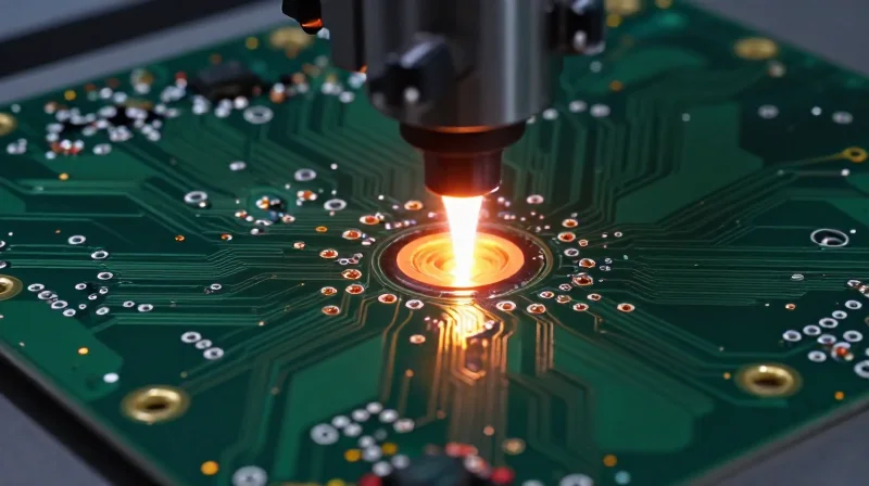
Precision Laser Ablation Protocols
Achieving reliable microvias in high-density interconnect (HDI) substrates for action cameras demands rigorous control over laser parameters. Modern CO2 and UV laser systems must be synchronized with specific material ablation thresholds to prevent thermal damage, such as carbonization or excessive glass-fiber protrusion within the dielectric stack.
Ablation Strategies for Ruggedized Reliability
| Laser Source | Primary Application | Advantage | Limitation |
|---|---|---|---|
| UV Laser | Copper/Resin Ablation | High precision, small via diameter | Slower processing time |
| CO2 Laser | Resin/Dielectric Removal | High throughput, clean wall geometry | Limited resolution on small pads |
Managing Aspect Ratios and Plating Integrity
In miniaturized circuitry, high aspect ratios (via depth vs. diameter) challenge the efficacy of subsequent electroless and electrolytic copper plating. To ensure void-free via filling, engineers must optimize the landing pad geometry and the plating chemistry agitation. For ruggedized applications, a 0.7:1 or lower aspect ratio is generally preferred to facilitate consistent copper coverage during the metallization phase.
- How do you mitigate glass-fiber protrusion?
Utilize laser systems with optimized pulse energy and frequency specifically tuned to the dielectric resin system, often paired with laser-direct imaging (LDI) to ensure precise alignment. - Why is aspect ratio critical for durability?
High aspect ratios lead to uneven plating deposition, resulting in structural weak points that can fracture under the thermal cycling or mechanical shock common in action camera environments. - What is the role of plasma desmear?
Plasma desmear is essential for cleaning the bottom of blind vias to ensure a robust electrical connection between layers, preventing inter-layer delamination during reflow.
Mastering Sequential Lamination for Multi-Layer Stacks
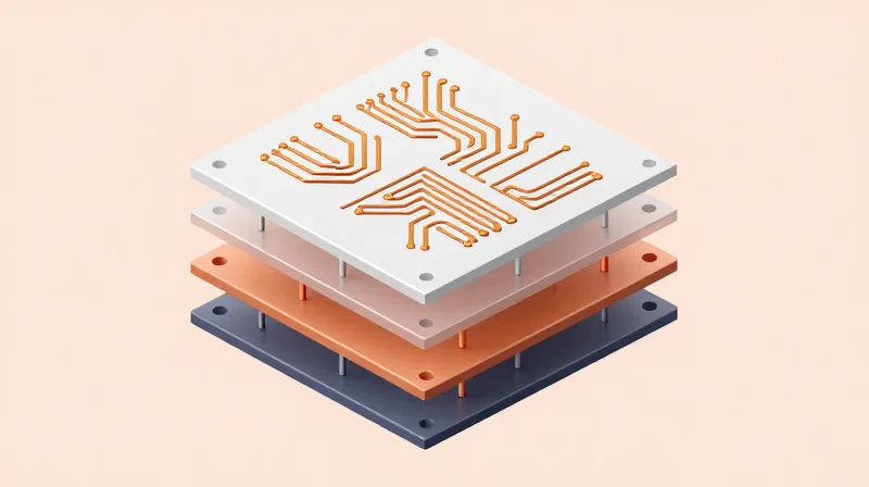
In the production of ruggedized action camera circuitry, sequential lamination serves as the foundational process for building high-density interconnect (HDI) stacks. As layer counts increase to support complex image processing and wireless modules, the mechanical stresses induced by temperature cycling during lamination pose a significant threat to via registration. Mastering this phase involves precise control over resin flow, CTE (Coefficient of Thermal Expansion) matching, and lamination pressure profiles to ensure structural integrity and signal reliability.
Optimizing Registration via Lamination Profiles
Registration errors are often the result of substrate movement caused by uncontrolled heat-up rates. To mitigate these effects, manufacturers must employ vacuum-assisted lamination with stepped temperature profiles. By balancing the ramp-up speed, engineers can manage the transition of the prepreg from a glassy state to a flowable state, significantly reducing the lateral shift of internal layers. Utilizing mechanical pin-lamination systems or X-ray alignment drilling post-lamination ensures that microvias remain perfectly centered within their target pads, even in thin, multi-layer HDI designs.
Comparison of Lamination Strategies for HDI
| Strategy | Registration Accuracy | Best For | Complexity |
|---|---|---|---|
| Mechanical Pin-Lam | High | Thick multi-layer | Moderate |
| Mass-Lam with X-Ray | Very High | Ultra-thin HDI | High |
| Sequential Build-Up | Moderate | Asymmetric stacks | High |
Addressing Common Lamination Challenges
- How do we prevent dielectric thickness variation?
Utilize low-flow prepregs and verify the resin content index before starting the press cycle to ensure uniform thickness across the panel. - Why does layer misalignment persist in sequential builds?
Usually, this stems from internal layer oxidation or excessive copper distribution asymmetry; balancing copper patterns on internal layers is vital for mechanical stability. - What is the impact of thermal shock on reliability?
Improperly cured resin systems can lead to delamination during reflow. Adhering to the manufacturer's recommended cure temperature profile is critical for long-term ruggedness.
Copper Balancing and Thermal Management
Mitigating PCB Warpage Through Copper Balancing
In HDI builds for action cameras, unsymmetrical copper distribution is the primary driver of structural deformation. During the lamination and reflow processes, mismatched coefficients of thermal expansion (CTE) between copper-dense and resin-rich zones create internal stresses. To maintain planarity, DFM engineers must enforce strict copper density targets, typically requiring a minimum of 40% and a maximum of 60% coverage across any given layer, with a specific focus on balanced patterns across the central axis of the PCB stackup.
| Design Factor | Action Camera Requirement | Result |
|---|---|---|
| Copper Distribution | Balanced (+/- 5%) | Reduced substrate bowing |
| Stackup Symmetry | Mirror-image layup | Zero neutral-axis drift |
| Trace Routing | Hatched copper planes | Improved thermal flow |
Thermal Management in Sealed Housings
Because action cameras utilize hermetically sealed or water-resistant enclosures, heat dissipation is almost entirely dependent on internal thermal paths. Utilizing micro-vias as thermal conduits is essential. By placing arrays of laser-drilled blind vias directly under high-heat processors (SoC) and power management ICs, designers can sink heat into internal ground planes or specialized copper heat spreaders, effectively bypassing the low thermal conductivity of standard FR-4 or high-Tg dielectric materials.
Frequently Asked Questions
- How does copper balancing affect high-frequency signal integrity?
Balanced copper prevents mechanical stress that can lead to micro-crack propagation in via barrels; by keeping the board flat, it ensures uniform dielectric thickness, which is essential for maintaining impedance control. - Can thermal vias create reliability issues during reflow?
Yes, if not properly plugged or capped with conductive epoxy. For HDI processes, we recommend copper-filled and capped (VIPPO) vias to prevent solder wicking and ensure a robust thermal interface to the heat spreader.
DFM Rules for High-Speed Signal Routing

DFM Rules for High-Speed Signal Routing
Achieving reliable high-speed data transmission in action cameras requires rigorous adherence to electromagnetic compatibility (EMC) standards within ultra-high-density footprints. Designers must prioritize strictly controlled impedance profiles and mitigate parasitic effects that compromise signal margins in compact, ruggedized environments.
Critical Design Requirements
- Impedance Consistency
Maintain a tolerance of +/- 5% for all differential pairs and high-speed single-ended traces by precise calculation of dielectric thickness and copper width. - Via Stub Mitigation
Implement back-drilling on high-frequency signals to eliminate unused via stubs, which act as resonant antennas and cause signal degradation above 5GHz. - Reference Plane Continuity
Ensure all high-speed traces are routed over a solid, unbroken ground reference plane; avoid splitting planes under signal paths to prevent impedance discontinuities. - Trace Geometry Rules
Use arc-based routing instead of 90-degree corners to reduce signal reflection and minimize EMI radiation at high clock speeds.
High-Speed Routing Comparison
| Parameter | Micro-stripline | Stripline |
|---|---|---|
| Location | Outer Layer | Inner Layer |
| EMI Shielding | Low | Excellent |
| Routing Complexity | Low | High (requires vias) |
| Signal Velocity | Faster | Slower (Dielectric load) |
Implementation Snippet
/* Example constraint for high-speed differential pairs */
Rule: DIFF_PAIR_IMPEDANCE = 90ohm +/- 5%;
Rule: MAX_VIA_STUB_LENGTH = 0.15mm;
Rule: MIN_COUPLING_DISTANCE = 3 * TraceWidth;
Rule: STACKUP_REFERENCE = 'GND_PLANE_L2';
Surface Finish and Solder Joint Reliability
Surface Finish Selection for High-Reliability HDI
In the context of ruggedized action cameras, the surface finish must provide more than just oxidation resistance; it must facilitate robust intermetallic compound (IMC) formation to endure extreme vibration and impact. For fine-pitch components on high-density interconnect (HDI) boards, the choice between Electroless Nickel Immersion Gold (ENIG) and Electroless Nickel Electroless Palladium Immersion Gold (ENEPIG) is central to preventing brittle failures like 'black pad' syndrome and ensuring long-term solder joint fatigue resistance.
| Surface Finish | Reliability Profile | Best Use Case |
|---|---|---|
| ENIG | Moderate | General HDI, standard consumer electronics |
| ENEPIG | Excellent | High-G environments, complex BGA assembly |
| Immersion Silver | Low | High-speed signal-sensitive boards, non-rugged |
Design Considerations for Solder Joint Integrity
- How does ENEPIG mitigate vibration-related failure?
The palladium layer in ENEPIG acts as a corrosion barrier for the nickel, preventing the formation of nickel-phosphorous corrosion (black pad) and ensuring a ductile, crack-resistant solder joint suitable for high-G mechanical shock. - Why should Solder Mask Defined (SMD) pads be used cautiously?
While SMD pads offer tighter registration for micro-vias, they can create stress concentration points. For ruggedized builds, Non-Solder Mask Defined (NSMD) pads are preferred where possible to allow better solder wrapping and mechanical locking. - What role does solder volume play in rugged designs?
Precise control of solder paste stencil thickness is required to avoid 'pillow-head' or head-in-pillow defects, which are notoriously difficult to detect and prone to intermittent failure under thermal cycling.
Beyond the finish, designers must utilize underfill materials for BGA and CSP components. Underfill serves as a mechanical buffer, distributing the G-forces exerted during camera impact away from the solder joints and into the board substrate itself. Combining ENEPIG finish with capillary underfill represents the gold standard for long-lifecycle action camera hardware.
Validation: Testing for Field Readiness
Accelerated Life Testing (ALT) and Environmental Stress
Validating ruggedized hardware requires pushing beyond standard operational limits to uncover latent failure modes in high-density interconnect (HDI) designs. For action cameras, the primary focus must be on combined mechanical and thermal stress, as high-frequency vibration coupled with fluctuating ambient temperatures often leads to solder fatigue and micro-via degradation.
| Stress Test | Key Parameter | Objective |
|---|---|---|
| Thermal Shock | -40°C to +85°C | Assess CTE mismatch between PCB dielectric and copper features. |
| Random Vibration | 10G to 20G RMS | Identify mechanical resonance and solder joint structural integrity. |
| High-Humidity Soak | 85% RH / 85°C | Evaluate moisture ingress prevention for HDI encapsulation. |
Validating Micro-Via Reliability
Micro-vias are the most vulnerable points in an HDI stack-up. To ensure long-term readiness, designers must implement cross-sectional analysis and interconnect stress testing (IST). IST is particularly effective for identifying barrel cracking or pad-to-trace separation before the design enters full-scale production.
Frequently Asked Validation Questions
- How many test cycles are required for thermal shock?
A minimum of 500 to 1,000 cycles is recommended for action camera certification to verify that CTE-induced stress does not initiate fracture in micro-via structures. - Is IST better than standard thermal cycling?
Yes; Interconnect Stress Testing (IST) allows for the precise, real-time monitoring of resistance changes in daisy-chained vias, providing data-driven insights into fatigue accumulation that standard oven testing cannot capture. - Why is vacuum-void inspection necessary for BGA components?
In high-vibration environments, even minor voids in solder joints can act as crack initiation sites. Maintaining a void ratio below 10% is essential for reliability in ruggedized optics.
Successfully deploying small-form-factor cameras into rugged environments relies on the intersection of precise DFM protocols and cutting-edge manufacturing techniques. By optimizing your HDI strategy early in the design cycle, you reduce development time and ensure total system reliability in the field. Contact our engineering team today to audit your current PCB designs and accelerate your time-to-market.
