
The demand for high-frame-rate, 8K resolution action cameras has outpaced the capabilities of traditional PCB designs. As thermal management and signal integrity become primary constraints, industry leaders are pivoting toward Micro HDI. This guide explores why this shift is non-negotiable for future rugged hardware.
The Evolution of Camera Hardware: Why Conventional PCBs Are Failing
The Bottleneck of Traditional Multilayer PCBs
Modern rugged imaging systems are no longer bound by simple optics but by the massive bandwidth required to process high-fidelity sensor data. Standard multilayer PCBs, characterized by their thicker substrates and reliance on traditional through-hole vias, are struggling to keep pace. These architectures introduce significant signal attenuation and electromagnetic interference, particularly as data rates move into the multi-gigabit per second (Gbps) range. For developers of industrial, aerospace, and defense imaging systems, the limitations are becoming critical.
Critical Performance Deficits
| Limitation Category | Standard Multilayer Impact | Operational Consequence |
|---|---|---|
| Signal Integrity | High Via Stubs/Inductance | Increased jitter and data packet loss |
| Thermal Management | Bulky Board Architecture | Localized hot spots near sensors |
| Spatial Efficiency | Large Component Pitch | Increased form factor, limited mobility |
Why HDI is the New Rugged Standard
Micro HDI (High-Density Interconnect) technology solves these issues by utilizing blind and buried microvias, significantly reducing trace lengths and parasitic capacitance. This architecture allows for thinner boards and more efficient routing, which is essential for the tight space constraints of modern rugged cameras. By shortening the signal path, Micro HDI minimizes the signal degradation that frequently plagues high-speed data transmission in harsh environments.
- How does Micro HDI improve thermal reliability?
Micro HDI allows for more efficient heat dissipation through optimized copper pour distribution and shorter thermal paths, reducing the temperature spikes seen at the sensor-to-PCB interface. - Does switching to Micro HDI increase production costs?
While unit costs for fabrication are higher, Micro HDI lowers total cost of ownership by increasing yield, reducing PCB size, and enhancing the longevity of components through improved signal stability.
Understanding Micro HDI (High Density Interconnect) Architecture
Defining Micro HDI Architecture
Micro High Density Interconnect (HDI) architecture is a refined fabrication method that utilizes advanced sequential lamination and laser-drilled microvias to achieve routing densities impossible with standard multilayer processes. By minimizing the footprint of interconnection points, designers can pack high-speed processing chips and image sensors into significantly smaller footprints without compromising thermal dissipation or signal bandwidth.
Mechanical vs. Laser-Drilled Vias
The primary differentiator in Micro HDI is the transition from mechanical drilling to laser ablation for via formation. Mechanical drills are limited by aspect ratios and drill bit breakage, which necessitates larger pad sizes to ensure electrical connectivity. Laser-drilled microvias allow for 'blind' and 'buried' configurations, which directly route signals between layers without occupying precious real estate on the board's surface.
| Feature | Standard Multilayer | Micro HDI |
|---|---|---|
| Via Type | Mechanical Thru-Hole | Laser-Drilled Microvia |
| Via Diameter | Greater than 200µm | Less than 100µm |
| Routing Space | Low Efficiency | High Density |
| Signal Integrity | Prone to Stub Effects | Optimized Impedance |
Key Advantages for Rugged Imaging
- How does Micro HDI improve signal integrity?
Microvias eliminate long via stubs that act as resonators in standard boards, significantly reducing signal reflection and EMI in high-bandwidth imaging data streams. - Why is this critical for ruggedized devices?
Lower mass and smaller surface area reduce the mechanical stress on solder joints during shock and vibration events, leading to a more reliable structural integrity. - Does it impact thermal performance?
Yes, Micro HDI allows for shorter electrical paths, which reduces resistive heating and facilitates more effective thermal management through strategic placement of copper-filled microvias.
Thermal Management and Power Density in Compact Form Factors
In the realm of rugged imaging, the convergence of high-speed processing and miniaturization creates a critical thermal bottleneck. Standard multilayer PCBs struggle to dissipate heat effectively due to their reliance on traditional through-hole vias, which occupy excessive board space and inhibit efficient thermal pathing. Micro HDI technology mitigates these issues by leveraging laser-drilled microvias that enable denser component placement while utilizing the copper-filled vias themselves as improved thermal conduits.
Thermal Dynamics in Hermetically Sealed Housings
Rugged imaging systems often operate in hermetically sealed environments where forced-air cooling is impossible. Consequently, the PCB must act as the primary heat spreader. Micro HDI architectures facilitate better thermal management through:
- Direct Thermal Pathing
Microvias can be placed directly underneath thermal pads (via-in-pad), providing a vertical thermal bridge to internal ground planes that standard through-hole designs cannot achieve. - Reduced Footprint
By eliminating large clearance requirements around mechanical drill holes, designers can achieve shorter trace lengths, reducing resistive heating and optimizing current distribution. - Optimized Copper Pour
Smaller interconnects allow for significantly higher copper density on inner layers, maximizing the total thermal mass available to absorb and distribute heat away from localized hotspots.
Comparing Thermal Efficiency and Density
| Metric | Standard Multilayer | Micro HDI |
|---|---|---|
| Via Diameter | 0.2mm - 0.3mm | 0.05mm - 0.1mm |
| Thermal Conductivity | Moderate (Via-limited) | High (Via-in-pad optimized) |
| PCB Density | Baseline | 3x to 5x Increase |
| Heat Spreading Efficiency | Restricted | Excellent |
Common Questions on HDI Thermal Performance
- Does high density increase the risk of localized overheating?
While component density is higher, the shortened thermal paths and improved copper volume in HDI stacks typically result in lower junction temperatures compared to traditional layouts. - How does HDI support power density in rugged cameras?
Micro HDI allows for sophisticated power distribution networks (PDN) that can handle higher current loads with less voltage drop, reducing the power loss that contributes to heat buildup.
Signal Integrity and High-Speed Data Throughput Challenges

The Physics of High-Speed Signal Degradation
As imaging sensors shift toward 4K and 8K resolutions at high frame rates, data throughput requirements have surged into the multi-gigabit per second range. In standard multilayer PCBs, long, serpentine routing traces act as antennas for electromagnetic interference (EMI) and suffer from significant signal attenuation due to skin effect and dielectric losses. Micro HDI technology mitigates these challenges by enabling tighter integration and shorter, direct signal paths.
Mitigating Parasitics with Microvias
Mechanical vias in standard PCBs create large parasitic capacitance and inductance, which act as impedance discontinuities for high-frequency signals. Micro HDI utilizes laser-drilled microvias, which are significantly smaller in diameter. This reduction in via barrel size minimizes the parasitic effect, ensuring consistent impedance control—crucial for maintaining signal fidelity in low-voltage differential signaling (LVDS) and MIPI CSI-2 interfaces.
| Feature | Standard Multilayer | Micro HDI |
|---|---|---|
| Via Diameter | 0.2mm - 0.3mm | < 0.1mm |
| Signal Path Length | Long/Meandering | Optimized/Direct |
| Parasitic Effect | High (Impedance Mismatch) | Low (Stable Integrity) |
| EMI Susceptibility | High | Negligible |
Frequent Questions Regarding HDI Implementation
- How do shorter trace lengths improve high-speed throughput?
Shorter traces reduce the length of the transmission line, minimizing resistive losses and the duration of signal exposure to ambient EMI, which preserves eye-diagram closure at high clock speeds. - Does Micro HDI improve signal routing density?
Yes, by utilizing microvias-in-pad and smaller line widths/spaces, designers can route high-speed buses directly under components, significantly reducing the routing complexity and PCB footprint. - Is impedance control easier with HDI?
HDI allows for finer control over stackup geometry and dielectric thickness, leading to more precise characteristic impedance (e.g., 50-ohm single-ended or 100-ohm differential) across the entire board.
Mechanical Resilience: Designing for High-Impact Rugged Environments
Structural Integrity Under High-G Loads
When subjected to high-acceleration environments—such as ballistic payloads or industrial vibration cycles—the mechanical weakness of a PCB often stems from solder joint fatigue and via-barrel cracking. Micro HDI technology mitigates these risks by utilizing staggered, laser-drilled microvias. Unlike traditional through-hole vias that act as structural 'perforations' across the entire board stack, microvias are shallower and confined to specific layers, significantly increasing the lateral rigidity of the substrate.
Substrate Material Selection
The choice of base materials determines how an imaging module survives thermal cycling and mechanical shock. High-Tg (glass transition temperature) laminates are essential for maintaining dimensional stability, preventing the dielectric from softening under extreme operating temperatures.
| Feature | Standard Multilayer | Micro HDI Technology |
|---|---|---|
| Via Reliability | High risk of barrel fracture | Low risk; stacked/staggered robustness |
| Board Flex | Higher due to large drill patterns | Lower due to reduced drill density |
| Solder Joint Stress | Higher due to component spacing | Minimized through optimal pad anchoring |
Frequently Asked Questions: Rugged Design
- How does HDI design prevent via-barrel cracking?
Laser-drilled microvias have a lower aspect ratio than mechanical drills, meaning the copper plating is more uniform and less susceptible to the stress concentrations that cause fatigue failures during high-g impacts. - Are there specific resins recommended for rugged imaging?
Yes, polyimide-based or reinforced ceramic-filled substrates are preferred for their superior mechanical strength and ability to maintain bond integrity under constant mechanical vibration.
Comparative Analysis: Micro HDI vs. Standard Multilayer Performance
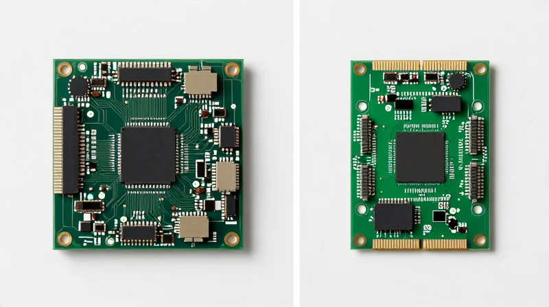
Comparative Performance Metrics
While standard multilayer PCBs remain a cost-effective solution for large-format imaging devices, Micro HDI technology has become the mandatory standard for miniaturized, high-performance rugged cameras. The transition to HDI is primarily driven by the need for increased functional density without compromising structural integrity under extreme mechanical stress.
| Metric | Standard Multilayer | Micro HDI |
|---|---|---|
| Board Space Efficiency | Moderate (Traditional routing) | Superior (Via-in-pad/Stacked vias) |
| Reliability (Thermal) | High (Stable expansion) | Excellent (Lower thermal impedance) |
| Signal Integrity | Subject to path loss | Optimal (Reduced parasitic capacitance) |
| Manufacturing Throughput | High (Proven process) | Lower (Complex multi-stage build) |
Key Trade-offs in Rugged Imaging Applications
- Why does Micro HDI perform better under vibration?
Micro HDI utilizes smaller, stacked laser-drilled vias which reduce the mechanical stress points typically found in large, through-hole standard vias, resulting in a more rigid and resilient interconnect structure. - How does integration density impact heat dissipation?
Despite higher component density, HDI allows for specialized thermal via arrays directly under heat-generating ICs, providing a more efficient conductive path for heat to reach the heat sink or chassis. - What is the primary manufacturing hurdle for HDI?
The sequential build-up process required for high-density interconnects introduces additional lamination cycles, which increases lead times and raises the cost per board compared to traditional multilayer manufacturing.
Ultimately, the choice between standard multilayer and Micro HDI rests on the specific SWaP-C (Size, Weight, Power, and Cost) requirements of the imaging platform. For mission-critical rugged devices where board real estate is at a premium and signal speeds exceed 5Gbps, Micro HDI provides the necessary technical advantage despite its more intensive fabrication requirements.
Manufacturing and Cost-Benefit Considerations
The Economic Trade-off: CAPEX vs. Lifecycle Reliability
The transition to Micro HDI technology represents a departure from traditional volume-based cost models. While standard multilayer boards benefit from mature, low-cost manufacturing processes, Micro HDI requires specialized laser-drilling capabilities and advanced material handling, resulting in higher initial fabrication costs. However, in the context of rugged imaging, the cost-benefit analysis must extend beyond the bill of materials. The reduction in failures, lower warranty claims, and decreased field maintenance cycles often justify the higher upfront investment by securing long-term product viability in mission-critical environments.
| Metric | Standard Multilayer | Micro HDI |
|---|---|---|
| Unit Cost | Low (Economies of Scale) | High (Advanced Fabrication) |
| Failure Rate | Moderate | Low (High Mechanical Integrity) |
| Design Complexity | Standard | High (Requires HDI Expertise) |
| Total Cost of Ownership | Moderate to High (due to maintenance) | Low (High Reliability Gains) |
Strategic Advantages for Rugged Imaging Manufacturers
Adopting Micro HDI is not merely a technical upgrade; it is a competitive differentiator. By shrinking board footprints, manufacturers can pack more sensors into smaller ruggedized enclosures, enabling a new generation of compact, high-performance imaging devices. This miniaturization, combined with the structural robustness provided by Micro HDI, allows companies to enter high-reliability markets—such as defense and industrial automation—where performance under pressure is the primary value driver.
Frequently Asked Questions
- Does the complexity of Micro HDI significantly increase time-to-market?
Initial design phases may be longer due to complex routing, but the high level of component integration often reduces final enclosure design time and mechanical assembly complexity. - When is it inappropriate to use Micro HDI for rugged applications?
If the application lacks space constraints and operates in benign environments, the added manufacturing costs and design lead-times of Micro HDI may not offer a sufficient return on investment compared to standard multilayer solutions. - Are there secondary cost savings with Micro HDI?
Yes, savings are often realized through reduced system size, simplified housing requirements, and improved signal integrity, which minimizes the need for complex, cost-heavy error correction circuitry.
Future-Proofing Your Imaging Hardware Roadmap
Strategic Evolution of Imaging Hardware
To future-proof imaging hardware roadmaps, engineering teams must move beyond legacy multilayer PCB designs, which often impose physical constraints that limit sensor integration and thermal management. Micro HDI (High-Density Interconnect) technology provides the necessary architecture to support smaller, more capable camera modules by allowing finer traces and higher via density, which are critical for high-speed signal integrity in 4K/8K imaging pipelines.
Comparative Roadmap Strategy
| Feature | Standard Multilayer | Micro HDI Integration |
|---|---|---|
| Component Density | Low/Moderate | High/Ultra-High |
| Signal Integrity | Prone to Crosstalk | Optimized via Stacked Vias |
| Ruggedization | High Mass/Volume | Low Profile/Compact |
| Thermal Pathing | Limited Efficiency | Enhanced Heat Dissipation |
Frequently Asked Questions
- Is Micro HDI cost-prohibitive for high-volume rugged cameras?
While initial NRE costs are higher, the reduction in board layers and improved production yield for complex circuits often results in lower total cost of ownership over a product's lifecycle. - How does Micro HDI improve signal integrity for sensors?
Micro HDI allows for shorter trace lengths and optimized return paths, significantly reducing EMI and noise interference essential for high-bit-depth image processing. - What is the primary risk of upgrading to Micro HDI?
The primary risk lies in manufacturing complexity; ensure your PCB fabrication partner has validated laser-drilling and plating processes for stacked micro-vias.
Engineering leaders should prioritize a modular design approach that allows for the integration of Micro HDI as the core backbone of their next-generation rugged chassis, ensuring physical space for battery life optimization and improved thermal mitigation.
Transitioning to Micro HDI is more than a design upgrade; it is a fundamental shift toward the reliability and performance required by modern action camera users. By adopting these advanced architectures, manufacturers can unlock new levels of durability and speed. Contact our engineering consulting team today to discuss how we can integrate Micro HDI into your next product design.
