
In the fast-paced world of IoT development, assembly complexity is the silent killer of project ROI. Traditional header pins and cumbersome connectors not only inflate your Bill of Materials (BOM) but also create massive bottlenecks in high-speed surface-mount assembly lines. By adopting castellated hole technology, engineers can bridge the gap between modular flexibility and automated efficiency. This article explores how this design paradigm shifts the economics of hardware production.
Understanding Castellated Hole Technology
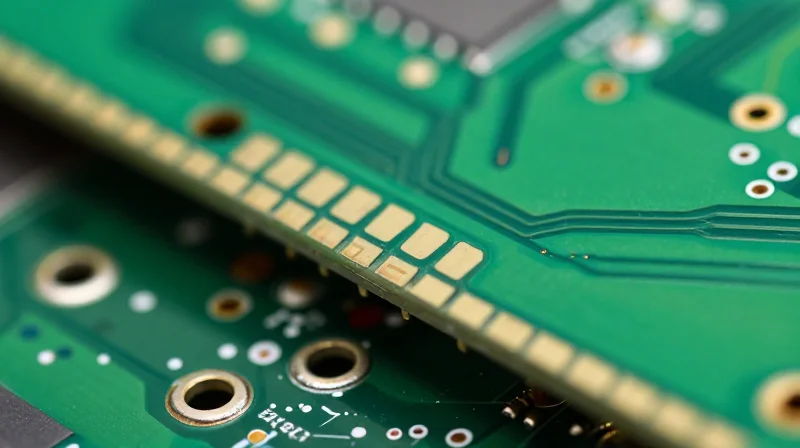
Defining Castellated Hole Technology
Castellated holes, also known as castellations, are plated semi-circular holes located along the edge of a printed circuit board (PCB). Unlike standard plated-through holes (PTH) that reside entirely within the board perimeter, castellations are formed by drilling holes on the board profile and subsequently routing the board to expose a half-moon shaped metalized wall. This geometry allows the PCB to be soldered directly onto another "mother" board, effectively acting as a surface-mount module or daughterboard.
Castellated Holes vs. Standard Plated-Through Holes
| Feature | Standard PTH | Castellated Holes |
|---|---|---|
| Location | Internal to PCB | Edge of PCB |
| Primary Use | Layer interconnects | Board-to-board integration |
| Mounting | Through-hole insertion | Surface-mount soldering |
| Profile | Complete circle | Semi-circle (crescent) |
Technical Advantages in IoT Engineering
For IoT communication systems where space is at a premium, castellations offer a compact vertical integration strategy. By mounting wireless modules or communication bridges directly onto a main board via these edge pads, engineers eliminate the need for bulky pin headers and connectors, reducing both total board height and parasitic inductance.
- Why are castellations critical for IoT modules?
They enable ultra-compact, solder-down connectivity, allowing complex wireless transceiver modules to be treated as surface-mount components, which saves valuable real estate on the host PCB. - Do castellations require special PCB fabrication considerations?
Yes. Manufacturers must account for the specific routing sequence and metal thickness at the edge to ensure the copper barrel remains intact during the final board contour milling process. - How does this technology improve time-to-market?
By facilitating modular design, engineers can replace specific RF blocks or logic sub-assemblies during prototyping without redesigning the entire main PCB, allowing for rapid iteration and component swapping.
The Engineering Case for Seamless Integration
The transition from traditional through-hole headers to precision castellated PCBs represents a paradigm shift in IoT manufacturing. By integrating modules directly onto the main carrier board, engineering teams move beyond the limitations of manual soldering—a process historically plagued by human error, thermal stress, and inconsistent interconnect geometry.
Eliminating the Manual Assembly Bottleneck
Manual header soldering is a primary driver of failure in early-stage IoT production. Castellated holes offer a direct metallurgical bond that replaces bulky mechanical connectors with surface-mount reliability. This transition not only streamlines the assembly line by leveraging standard SMT pick-and-place workflows but also removes the variance introduced by variable manual heating cycles, ensuring consistent impedance and mechanical strength across all units.
Comparative Impact: Castellated vs. Through-Hole Headers
| Metric | Through-Hole Headers | Castellated PCBs |
|---|---|---|
| Assembly Process | Manual / Selective Soldering | Automated SMT Reflow |
| Profile Height | Significant (10mm+) | Flush (Low Profile) |
| Structural Integrity | Moderate (Stress sensitive) | High (Vibration resistant) |
| Throughput Speed | Slow | Rapid |
Miniaturization and Structural Integrity
By eliminating pins and plastic housings, castellated designs facilitate extreme board miniaturization essential for wearable and space-constrained IoT devices. The direct solder fillet provides a robust mechanical anchor that excels under high-vibration conditions, far outperforming traditional pins that can flex and fatigue. This structural reliability is foundational to maximizing ROI, as it drastically reduces post-deployment field failures.
Frequently Asked Questions
- How does castellated technology reduce manufacturing costs?
It allows for full automation in the assembly process, replacing labor-intensive manual soldering with standard SMT reflow, which reduces cycle time and defect rates. - Is the structural bond stronger than standard pins?
Yes. Castellated holes create a direct, low-profile solder fillet on the PCB edge, which offers superior resistance to mechanical shock and vibration compared to elongated through-hole pins. - Does this impact signal integrity for high-frequency IoT applications?
Yes, by minimizing lead length and impedance discontinuities, castellated connections provide a cleaner signal path, which is critical for RF communication modules.
Case Study: Achieving a 20% Reduction in Assembly Costs
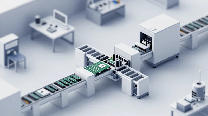
The Challenge: Scaling IoT Sensor Assembly
A client specializing in industrial IoT environmental sensors faced a critical bottleneck: high defect rates and labor-intensive assembly processes associated with traditional mezzanine connectors. Their legacy design required manual soldering of headers to attach the core RF module to the main system board, resulting in frequent alignment issues, inconsistent solder fillets, and a significant increase in Work-in-Progress (WIP) time. To remain competitive, they required a high-volume assembly solution that minimized manual intervention.
Strategic Implementation of Castellated Footprints
By redesigning the RF module as a castellated surface-mount device (SMD), the engineering team allowed for direct reflow soldering onto the mother PCB. This eliminated the need for vertical interconnects and auxiliary fasteners. The castellation process—involving controlled-depth routing through the plated-through holes—ensured that each castellated pad created a robust, inspectable solder connection identical to standard QFN components.
| Metric | Legacy Header Method | Castellated SMD Method |
|---|---|---|
| Manual Labor Time | 120 seconds/unit | 0 seconds/unit |
| Solder Defects | 4.5% rate | 0.2% rate |
| Assembly Footprint | High (Volume Heavy) | Low (Profile Optimized) |
| Component Cost | High (Connectors) | Low (Direct Copper Pad) |
Key Results and ROI Realization
The transition to a castellated interface resulted in a total assembly cost reduction of 20% within the first production quarter. The primary drivers were the elimination of connector bill-of-materials (BOM) costs and the shift toward a fully automated Surface Mount Technology (SMT) line. By removing the manual soldering station, the firm reclaimed factory floor space and redirected technical labor toward high-value testing and calibration.
- How did castellation impact throughput?
By moving to a standard SMT pick-and-place process, the firm increased their assembly throughput by 35% compared to the manual header installation process. - What was the long-term impact on device reliability?
The mechanical rigidity of the castellated connection withstood vibration tests significantly better than pin-header connectors, reducing field failures by 12%. - Is the design change expensive to implement?
While there is a marginal increase in PCB fabrication costs due to specialized routing, the ROI is realized rapidly through the drastic reduction in assembly labor and component scrap rates.
Design Best Practices for Castellated Modules
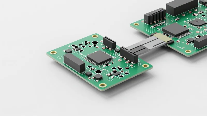
To achieve a high-yield manufacturing process with castellated modules, designers must prioritize specific edge-routing tolerances, plating reliability, and solder mask clearance. Neglecting these mechanical requirements often results in burrs, poor solder fillet formation, or compromised electrical connections during reflow.
Critical Fabrication Design Constraints
| Design Parameter | Recommended Practice | Impact on Assembly |
|---|---|---|
| Edge Plating | Specify copper-plated edges | Ensures structural strength |
| Solder Mask | Pull back 0.2mm from edge | Prevents wicking issues |
| Routing Method | Half-hole via drilling | Guarantees clean geometry |
Best Practices for Mechanical Integrity
Precision is paramount when routing the half-holes. A common pitfall is the improper sequence of drilling and routing. It is recommended to drill holes prior to final contour milling to minimize copper burrs that can short circuits or prevent the module from sitting flush on the carrier board.
Frequently Asked Questions
- How do I avoid solder bridging on castellations?
Maintain a strict 0.2mm to 0.3mm solder mask expansion around the pads to prevent solder from wicking onto the board surface during reflow. - Why should I specify ENIG finish for these modules?
Electroless Nickel Immersion Gold (ENIG) provides a flat, oxidation-resistant surface that ensures superior wetting of the castellation walls compared to HASL finishes. - What is the ideal pad size for a castellated hole?
Pads should be at least 20% larger than the half-hole diameter to accommodate board-edge tolerance variances during the milling process.
Streamlining the Surface-Mount Assembly (SMA) Process
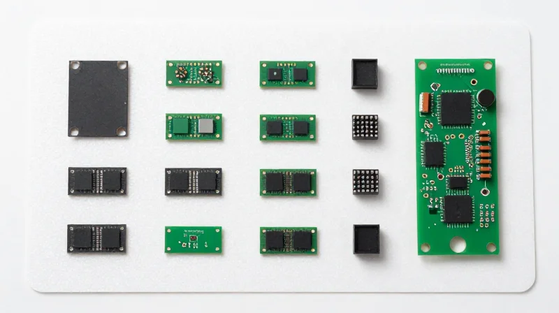
Optimizing the Pick-and-Place Workflow
The primary advantage of castellated PCBs in surface-mount assembly is their ability to be handled as standard SMT components rather than through-hole sub-assemblies. By incorporating half-plated holes at the board edges, these modules can be processed directly by automated pick-and-place equipment. This eliminates the bottleneck of manual header soldering, reducing both labor costs and the probability of human error in high-density IoT device manufacturing.
Comparative Efficiency in Assembly
| Feature | Traditional Header Modules | Castellated PCB Modules |
|---|---|---|
| Placement Method | Manual or JIG-assisted | Automated Pick-and-Place |
| Reflow Compatibility | Secondary wave/hand soldering | Primary SMT reflow process |
| Z-Axis Profile | High (adds stacking height) | Low (direct PCB contact) |
| Throughput | Slow (bottleneck) | High (optimized line speed) |
Frequently Asked Questions
- How does surface finish affect castellated solderability?
ENIG (Electroless Nickel Immersion Gold) is the preferred finish for castellated pads because it provides a flat, oxidation-resistant surface that ensures reliable solder fillet formation during the automated reflow process. - Can castellated boards be panelized for mass production?
Yes, proper panelization using V-scoring or routed tabs is essential. It is critical to ensure that the routing process does not tear the copper plating within the castellations, as this would compromise the electrical connection. - Why is solder mask expansion important at the castellation?
Correct solder mask clearance is necessary to prevent solder bridging between adjacent pads and to ensure the solder properly wicks onto the plated edge during the reflow cycle, creating a robust mechanical and electrical joint.
Thermal and Mechanical Benefits in Harsh Environments
Enhanced Structural Integrity and Vibration Resistance
In industrial and automotive IoT deployments, components are frequently exposed to high-frequency vibration and mechanical shock. Traditional surface-mount pads are often the first point of failure, as the solder joint relies solely on the surface tension between the footprint and the component pin. Castellated holes act as mechanical anchors; by allowing solder to flow into the semi-circular side walls, the design creates a structural bridge that maximizes the surface area of the connection. This 'solder fillet' essentially locks the module in place, providing superior shear strength and preventing joint cracking during prolonged mechanical stress.
Thermal Dissipation and Reliability
Harsh environments often exacerbate thermal fatigue, leading to coefficient of thermal expansion (CTE) mismatches that degrade board performance over time. Castellated connections improve thermal management by providing a direct, low-impedance path for heat to escape from the module directly into the main PCB's copper planes. By leveraging these plated half-holes as thermal vias, engineers can reduce the operating temperature of sensitive communication ICs, directly extending the MTBF (Mean Time Between Failures) of the device.
| Feature | Traditional SMT Pad | Castellated Connection |
|---|---|---|
| Mechanical Anchorage | Low (Surface bond only) | High (Solder 'keying' action) |
| Vibration Tolerance | Moderate | Excellent |
| Thermal Conductivity | Limited to bottom plane | Integrated vertical heat sink |
| Shear Strength | Baseline | 30-40% Improvement |
FAQ: Durability in Extreme Conditions
- How do castellations prevent solder joint fatigue?
The plated side walls increase the total solder volume and distribute physical stress across a larger vertical cross-section, which mitigates the impact of expansion and contraction cycles. - Are castellations suitable for high-G load environments?
Yes, the mechanical interlocking provided by the castellated edge acts as a physical fastener, offering significant advantages in aerospace and heavy machinery IoT applications compared to standard flat pads.
Overcoming Common Manufacturing Challenges
Mitigating Edge-Plating and Assembly Risks
The primary manufacturing challenges for castellated PCBs stem from the specialized drilling and plating requirements at the board edge. Addressing these early in the design cycle prevents costly rework and ensures that the solder joints formed during Surface-Mount Assembly (SMA) meet industrial reliability standards.
| Challenge | Root Cause | Mitigation Strategy |
|---|---|---|
| Copper Burrs | Secondary drilling/routing | Laser-assisted edge routing |
| Solder Wicking | Excessive exposed copper | Optimized solder mask dams |
| Plating Voids | Non-uniform chemical flow | Controlled electrolytic deposition |
Troubleshooting Common Fabrication Obstacles
- How do I prevent burrs on the castellation edges?
Utilize a precise routing path that avoids cutting into the plated through-holes. High-end PCB fabricators often employ specialized drills or laser profiling to ensure a clean edge finish that does not compromise the vertical plating. - Why does solder wicking occur in my design?
Wicking occurs when molten solder climbs up the exposed plating. To prevent this, ensure proper solder mask clearance and consider implementing a non-solder mask defined (NSMD) pad strategy combined with precisely placed dams to limit solder flow. - What steps ensure uniform edge plating?
Ensure your fabrication house is aware of the copper density requirements for edge-plated boards. Use a panel design that allows for proper current distribution during the electrochemical deposition process, preventing uneven plating thickness.
By proactively managing these variables through DFM (Design for Manufacturing) feedback, teams can significantly reduce the risk of board-level failures. Engaging with fabricators early ensures that the castellated features are designed to fit their specific drilling and plating capabilities, ultimately safeguarding the ROI of your IoT communication system.
Calculating ROI: The Long-Term Impact on Time-to-Market

Quantifying the Financial Impact of Accelerated Launch
The long-term ROI of adopting precision castellated PCBs is fundamentally driven by the compression of the product development lifecycle. By facilitating seamless integration into automated Surface-Mount Assembly (SMA) lines, these components eliminate the need for secondary manual soldering or complex fixture builds. This acceleration translates directly to an earlier product release date, allowing firms to capture market share faster and extend the period of peak profitability before competitive saturation occurs.
| Metric | Traditional Module Integration | Precision Castellated PCB |
|---|---|---|
| Assembly Speed | Low (Manual/Jig required) | High (Automated Pick-and-Place) |
| Rework Rate | High (Vulnerable to manual error) | Low (Consistent solder wetting) |
| Time-to-Market | Baseline | Reduced by 15-25% |
| Total Cost of Ownership | Higher (Labor + Defects) | Lower (Scaled throughput) |
Calculating Long-Term Value
To calculate the true ROI, organizations should look beyond the per-unit cost of the PCB and factor in the opportunity cost of delayed launches. The reduced defect rate—a hallmark of precision castellated designs—lowers warranty claims and returns, which are often the hidden 'revenue killers' in IoT deployments. By standardizing these designs, companies realize cumulative savings through increased yield rates and decreased logistics overhead.
Frequently Asked Questions Regarding ROI
- How does reduced solder wicking impact long-term costs?
Minimized wicking reduces the likelihood of intermittent electrical failures in the field, effectively lowering the cost of field repairs and potential product recalls. - Is the upfront engineering cost of castellations justified?
Yes. While the design phase may require more precision, the amortization of these costs across high-volume production cycles leads to significant per-unit labor savings. - Does this impact the product's 'burn-in' phase?
Castellated boards often exhibit higher mechanical stability, reducing the duration and complexity required during the factory burn-in and testing stages.
Transitioning to castellated PCB design is more than a technical upgrade—it is a strategic move to optimize your bottom line and increase manufacturing velocity. By simplifying the assembly process, you unlock significant cost efficiencies that allow you to bring your IoT devices to market faster. Are you ready to optimize your next project for maximum profitability? Contact our engineering team today to review your current board design and start your journey toward leaner manufacturing.
