
In the precision-driven world of In-Vitro Diagnostics (IVD), the smallest signal fluctuation can translate into significant clinical errors and operational downtime. As hardware complexity increases, the integrity of your PCB design is no longer just a technical hurdle—it is a critical business metric. This article explores how advanced PCB stack-up optimization acts as a primary lever for maximizing hardware ROI and ensuring long-term system reliability.
The Direct Link Between Signal Integrity and IVD Precision

The Direct Link Between Signal Integrity and IVD Precision
In the realm of In-Vitro Diagnostics (IVD), the integrity of low-voltage analog signals is the primary arbiter of diagnostic precision. Because diagnostic sensors—such as those used in fluorescence detection, electrochemical biosensors, or impedance spectroscopy—operate at microvolt or picoampere scales, even minor electromagnetic interference (EMI) or signal degradation caused by substandard PCB fabrication can be indistinguishable from actual biological data. When signal noise compromises the signal-to-noise ratio (SNR), the hardware effectively masks subtle analytical shifts, leading to increased false-positive rates, reduced sensitivity, and the inability to detect low-abundance biomarkers.
Mechanisms of Signal Corruption
| Noise Source | PCB Manufacturing Factor | Impact on Diagnostic Output |
|---|---|---|
| Crosstalk | Improper trace spacing & coupling | Artifacts in parallel sensor channels |
| Ground Bounce | Inadequate impedance control | Instability in reference voltages |
| EMI Susceptibility | Insufficient layer shielding | Baseline drift in detection threshold |
Optimizing the physical manufacturing process—specifically regarding stack-up configuration, trace impedance precision, and via-in-pad reliability—is not merely a design preference; it is a manufacturing imperative to safeguard biological data integrity and improve the overall ROI of the diagnostic platform.
Frequently Asked Questions on Signal Fidelity
- How does PCB manufacturing variance impact clinical results?
Manufacturing deviations in trace width and dielectric constant alter the impedance profile of signal lines, introducing reflection noise that can distort high-speed analog-to-digital conversion, directly impairing the system's Limit of Detection (LOD). - Can firmware compensate for poor PCB-level signal integrity?
While digital signal processing (DSP) can filter some noise, it often introduces latency or risks masking low-level diagnostic signals. It is mathematically and economically superior to eliminate noise at the hardware layer rather than relying on aggressive digital post-processing.
Understanding the Anatomy of PCB Stack-Up Optimization
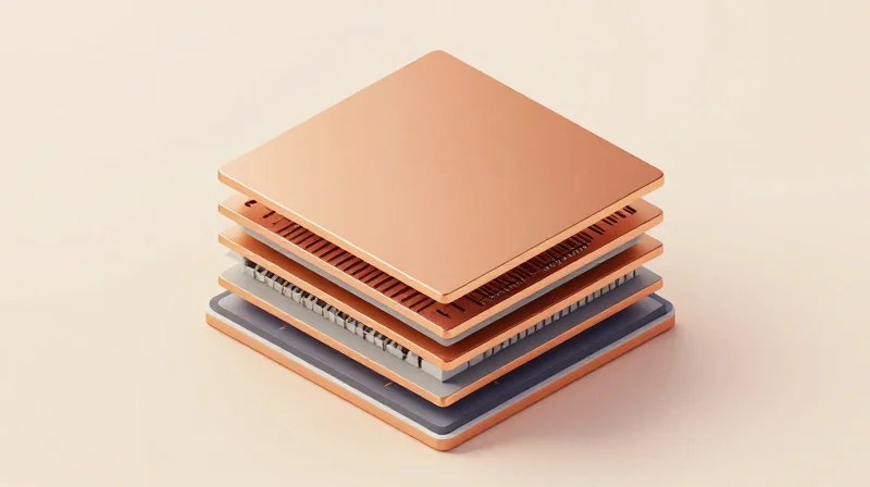
In the context of sensitive diagnostic hardware, the PCB stack-up is not merely a mechanical support structure but an integral component of the electronic system's signal transmission performance. Strategic layer management reduces crosstalk, suppresses common-mode noise, and facilitates controlled impedance, all of which are essential for maintaining the sub-microvolt precision required in diagnostic measurements.
Core Principles of Stack-Up Design
To achieve superior signal integrity, engineers must prioritize the proximity of signal layers to ground planes. A tighter coupling reduces the loop area through which electromagnetic fields propagate, thereby minimizing radiated emissions and susceptibility to external noise.
| Design Factor | Impact on Signal Integrity | Optimization Strategy |
|---|---|---|
| Layer Spacing | High loop inductance | Use thin prepreg for closer coupling |
| Return Path | Signal distortion | Ensure continuous solid ground planes |
| Impedance | Signal reflections | Match trace width and dielectric constant |
Frequently Asked Questions
- Why is layer symmetry critical in diagnostic boards?
Symmetrical stack-ups prevent mechanical warping during the lamination process and ensure that thermal coefficients are balanced, maintaining consistent dielectric spacing across the board. - How does impedance control minimize noise?
Controlled impedance prevents signal reflections at trace discontinuities, ensuring that energy is delivered to the load rather than oscillating back to the source as noise. - What is the role of burial vias in noise reduction?
Buried and blind vias minimize the antenna effect caused by long, unused via stubs, which otherwise act as resonators for high-frequency interference.
Minimizing Hardware Failure Rates through Design Integrity
The operational lifespan of diagnostic hardware is fundamentally tied to the structural integrity of its printed circuit board (PCB) assemblies. When design choices fail to account for thermal expansion, voltage spikes, or electromagnetic noise, the resulting stress leads to premature component degradation, intermittent connectivity, and costly field failures. By optimizing board layouts to minimize these stresses, manufacturers ensure that sensitive diagnostic instruments maintain clinical precision throughout their service life.
Mitigating Thermal Fatigue via Material Selection
Thermal cycling is the primary driver of solder joint fatigue in high-performance diagnostic units. Integrating thermally stable materials and optimizing the distribution of high-heat components prevents localized board warping. When the coefficient of thermal expansion (CTE) is mismatched between layers, the resulting mechanical strain often causes micro-cracking in vias and traces, leading to unpredictable signal loss.
| Design Strategy | Impact on Hardware Reliability | ROI Benefit |
|---|---|---|
| Thermal Vias Placement | Dissipates heat from sensitive ICs | Reduced field replacement costs |
| Controlled CTE Materials | Prevents structural micro-cracks | Extended instrument lifespan |
| Advanced EMI Shielding | Stabilizes low-voltage signals | Fewer software-level error reports |
Electrical Noise and Component Longevity
Unfiltered electrical noise acts as a cumulative stressor on board components. When noise is not addressed at the routing level, it creates voltage transients that exceed component thresholds, accelerating the wear of sensitive diagnostic sensors. Precise impedance control and the strategic use of decoupling capacitors act as a buffer, smoothing power delivery and preventing the cascading failures that plague unoptimized hardware.
Frequently Asked Questions on Hardware Reliability
- How does signal noise cause hardware failure?
Persistent electrical noise creates voltage stress on components beyond their design specifications, leading to accelerated electrolytic capacitor degradation and semiconductor breakdown. - Does PCB stack-up design impact repair costs?
Yes. A well-engineered stack-up reduces electromagnetic interference, which lowers the rate of 'no-fault-found' (NFF) service calls that often occur when noise is mistaken for component failure. - What is the most critical design factor for reducing failure rates?
Prioritizing thermal management, specifically by balancing copper distribution and utilizing thermal reliefs, is the most effective way to prevent long-term mechanical failure of PCB interconnections.
Enhancing Equipment Longevity and Field Lifecycle
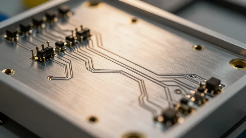
Extending Operational Longevity Through PCB Integrity
Optimizing PCB manufacturing goes beyond immediate signal fidelity; it directly impacts the physical endurance of diagnostic equipment. By implementing robust stack-up configurations and selecting materials with superior thermal coefficients, manufacturers can reduce mechanical fatigue caused by repeated power cycling and environmental shifts. This proactive design philosophy minimizes the degradation of vias and trace adhesion, ultimately lengthening the MTBF (Mean Time Between Failures) and reducing the frequency of costly field maintenance interventions.
Comparative Impact of Manufacturing Choices
| Design Factor | Standard Approach | Advanced Optimization | Lifecycle Benefit |
|---|---|---|---|
| Substrate Material | Standard FR-4 | High-Tg Polyimide | Reduced thermal expansion fatigue |
| Copper Weight | Standard 0.5 oz | Increased 1-2 oz | Lower resistive heat generation |
| Surface Finish | HASL | ENEPIG | Enhanced corrosion and wear resistance |
Frequently Asked Questions
- How does signal noise reduction impact physical board life?
Reduced signal noise often indicates better impedance control and thermal management, which prevents localized 'hot spots' that contribute to the long-term degradation of board materials and electronic components. - Does advanced stack-up design increase manufacturing costs?
While unit costs may rise due to higher-grade materials or complex layer management, the total cost of ownership decreases significantly through reduced field service calls and extended asset replacement cycles. - Why is ENEPIG surface finish preferred for high-reliability diagnostics?
ENEPIG offers superior oxidation resistance and mechanical reliability compared to standard solder finishes, making it ideal for systems that must operate reliably in challenging clinical environments for several years.
The Financial Impact: Cost-Benefit Analysis of Advanced Manufacturing
The Economic Calculus of Signal Integrity
Transitioning from standard FR-4 manufacturing to high-integrity stack-ups and advanced material sets represents a shift from capital-intensive repair cycles to long-term reliability dividends. While optimized manufacturing processes increase unit costs by 15-25%, the mitigation of signal-to-noise ratio (SNR) issues drastically reduces post-production rework, field warranty claims, and diagnostic re-testing requirements.
| Metric | Standard Manufacturing | Optimized PCB Design |
|---|---|---|
| Unit Production Cost | Baseline ($) | Baseline + 20% |
| Field Failure Rate | 3.5% | 0.8% |
| Signal Re-testing Frequency | High | Negligible |
| Warranty Liability | High | Low |
Quantifying ROI through Lifecycle Savings
The ROI of advanced PCB manufacturing is best viewed through the lens of Total Cost of Ownership (TCO). By investing in precision impedance control and low-loss substrates, manufacturers eliminate intermittent signal noise that often triggers false diagnostic positives. This reduction in 'false failures' prevents unnecessary shipping and service labor costs, which typically outweigh the initial bill-of-materials increase within the first six months of deployment.
Frequently Asked Questions
- Does advanced manufacturing always increase the upfront cost?
While materials like high-Tg resins or specialized laminates are more expensive, optimization of the stack-up can often reduce layer counts or eliminate the need for expensive external shielding, potentially offsetting the unit cost. - How does signal noise reduction specifically impact ROI?
Signal noise reduction decreases data corruption and calibration errors, reducing the frequency of field recalls and extending the interval between calibration service visits, directly lowering operational expenditure. - What is the primary indicator of a successful financial transition to advanced design?
The primary indicator is a measurable decline in 'No Fault Found' (NFF) service returns, which are the most costly and inefficient category of hardware support.
Data Reliability as a Competitive Advantage
The Clinical Value of Noise-Free Data
In the highly competitive diagnostic hardware market, data reliability is not merely a technical specification; it is the fundamental driver of clinical adoption. When manufacturing optimization reduces signal noise, diagnostic equipment achieves lower False Discovery Rates (FDR) and higher Sensitivity and Specificity. This reliability transforms hardware from a commodity into a trusted clinical partner, directly influencing procurement decisions in hospitals where diagnostic speed and accuracy are paramount.
Impact Analysis: Standard vs. Optimized Manufacturing
| Metric | Standard PCB Design | Optimized PCB Design |
|---|---|---|
| Signal-to-Noise Ratio (SNR) | Baseline/Variable | High/Consistent |
| Clinical Confidence | Moderate | High |
| Diagnostic Artifacts | Frequent | Negligible |
| Market Positioning | Budget-Tier | Premium/Reliable |
Strategic Differentiation Through Hardware Integrity
Manufacturers that prioritize signal integrity at the PCB level create a defensible moat against competitors. By utilizing advanced materials and optimized stack-ups, vendors can guarantee data consistency across varied environments. This reliability mitigates the risk of diagnostic errors, which protects the manufacturer's brand reputation and significantly lowers liability costs, providing a long-term return on investment that outweighs the initial manufacturing premium.
Frequently Asked Questions
- How does signal noise impact clinical workflow?
Excessive noise causes diagnostic artifacts, requiring clinicians to perform repeat scans, which increases patient wait times and reduces overall clinic throughput. - Can PCB manufacturing choices be used as a marketing tool?
Yes, by demonstrating higher SNR and data repeatability, manufacturers can provide evidence-based claims that help hospital procurement teams justify higher capital investments. - Does noise reduction influence diagnostic software performance?
Clean hardware signals reduce the burden on post-processing algorithms, leading to faster image reconstruction and more accurate AI-driven diagnostics.
Best Practices for Collaborative Engineering
Bridging the Design-to-Manufacturing Gap
To achieve superior signal integrity in diagnostic hardware, engineers must transition from isolated design workflows to integrated manufacturing partnerships. When signal noise is treated as a downstream manufacturing problem rather than a core design constraint, ROI suffers due to repeated prototyping cycles and performance degradation.
Critical Collaboration Frameworks
- Early-Stage Manufacturability Reviews
Engage manufacturing partners during the schematic phase to identify potential impedance discontinuities that could amplify noise in sensitive sensor arrays. - Standardized Stack-up Documentation
Provide precise dielectric constant requirements and copper weight specifications to prevent variance between the simulation model and the physical product. - Material Selection Alignment
Collaborate on material selection (e.g., high-Tg resins or low-loss laminates) to ensure signal loss profiles remain within tight tolerances for high-frequency diagnostics.
Collaboration Efficiency Comparison
| Engagement Strategy | Signal Noise Risk | Typical ROI Impact |
|---|---|---|
| Siloed Design (Throw-over-the-wall) | High | Negative (Rework & Delays) |
| Partial Review (Post-Layout) | Moderate | Neutral (Standard Yield) |
| Integrated Co-Design | Low | Positive (First-Pass Success) |
Ensuring Data Integrity
To maintain the highest standards of diagnostic accuracy, engineering teams must establish shared data validation protocols. This includes automated DFM (Design for Manufacturing) feedback loops that check trace width, spacing, and via structures against the fabricator’s unique process capabilities. By treating the manufacturing partner as a technical consultant, firms reduce the statistical likelihood of signal interference that often emerges from 'best-effort' generic production standards.
Future-Proofing Your Diagnostic Platform
Designing for Long-Term Scalability
To ensure diagnostic hardware remains relevant as testing requirements evolve, engineers must transition from static designs to adaptable, high-integrity platforms. Future-proofing centers on the implementation of advanced materials and high-density interconnect (HDI) technologies that accommodate increased signal processing needs without introducing noise or thermal instability.
Strategic Optimization Levers
| Strategy | Future-Proofing Benefit | Impact on ROI |
|---|---|---|
| Modular RF Front-Ends | Allows for rapid sensor upgrades without PCB redesign. | Reduces long-term CAPEX. |
| Controlled Impedance Vias | Supports higher data throughput for complex assays. | Extends product lifespan. |
| Advanced Thermal Vias | Enables miniaturization of high-throughput hardware. | Reduces field maintenance costs. |
Frequently Asked Questions
- How does PCB manufacturing optimization impact future clinical requirements?
Optimizing signal noise floors now allows for the later integration of more sensitive, high-throughput biosensors that would otherwise fail on noisier, standard-process boards. - Can I upgrade my current board design without a complete overhaul?
By adopting a 'design-for-modularity' approach, you can isolate sensitive analog paths, allowing for drop-in replacements of digital control logic as processing power requirements scale. - Is the investment in advanced PCB manufacturing worth the premium?
The ROI is realized through the reduction of field failures, extended hardware service cycles, and the ability to pivot to new diagnostic modalities without re-engineering the entire electronic architecture.
Optimizing your PCB stack-up is an investment in both your brand’s reputation and your bottom line. By prioritizing signal integrity, you minimize costly hardware failures and deliver the consistent, accurate results that clinicians demand. Ready to elevate your diagnostic hardware performance? Contact our engineering team today to review your current designs and uncover opportunities for optimization.
