
In the world of In-Vitro Diagnostics (IVD), the difference between a life-saving diagnosis and a false result often lies at the microscopic level of the PCB. When working with ultra-low signals, even the slightest noise or manufacturing variance can compromise system accuracy. Engineering managers face the daunting task of identifying suppliers who can translate high-precision designs into reliable hardware. This guide provides the strategic framework needed to vet manufacturing partners who possess both the technical capability and the regulatory rigor required for high-stakes medical instrumentation.
Understanding the Unique Challenges of Low-Signal IVD Equipment

Low-signal in-vitro diagnostic (IVD) systems operate at the edge of the physical noise floor. Because these instruments detect minute changes in electrochemical potentials or optical intensity, any manufacturing imperfection—from trace geometry variations to dielectric inconsistencies—can amplify noise, resulting in inaccurate patient results. Understanding the physics behind these sensitivities is the first step in selecting a manufacturing partner capable of maintaining signal integrity.
The Triad of Signal Degradation
| Challenge | Physical Root Cause | Impact on IVD Systems |
|---|---|---|
| EMI Sensitivity | Lack of board-level shielding and trace loops | Artifacts in raw readings and false positives |
| Thermal Noise | High ESR in copper paths and uneven heat dissipation | Voltage drift in analog-to-digital converters |
| Impedance Mismatch | Controlled impedance deviation in manufacturing | Signal reflections in high-frequency sensor interfaces |
Why Manufacturing Precision Matters for Low-Voltage Readings
In low-signal IVD instrumentation, the signal-to-noise ratio is often compromised by the PCB substrate itself. Variations in dielectric constant (Dk) across the board can cause localized impedance swings, while trace thickness tolerances affect the resistance of delicate signal paths. When manufacturing processes do not maintain tight control over these variables, the resulting inconsistencies introduce thermal noise and phase shifts that software-based filtering cannot fully recover.
Frequently Asked Questions
- How does trace impedance affect IVD sensitivity?
Impedance mismatch creates signal reflections that interfere with the primary diagnostic signal, effectively masking the low-voltage data points needed for accurate quantification. - Why is thermal stability critical for PCB substrate selection?
Thermal expansion and contraction can physically shift copper traces, changing the parasitic capacitance and inducing measurable voltage drift in highly sensitive analog instrumentation. - What manufacturing metric is most important for low-signal boards?
Controlled impedance and layer-to-layer registration accuracy are the most critical metrics, as they ensure consistent signal paths and optimal ground-plane coupling.
The Non-Negotiable: Verifying ISO 13485 and Regulatory Compliance
For manufacturers of IVD instrumentation, selecting a PCB partner is not merely a supply chain decision; it is an extension of your own regulatory umbrella. In the highly regulated medical device landscape, compliance is non-negotiable. If a PCB manufacturer cannot demonstrate rigorous adherence to ISO 13485 standards, they introduce unacceptable risk to your product's certification pathway, market readiness, and patient safety.
ISO 13485: The Gold Standard for Medical PCB Production
ISO 13485 is the internationally recognized quality management system (QMS) standard for the medical device industry. Unlike general manufacturing standards, it focuses heavily on risk management, traceabilty, and documented consistency. For a PCB fabricator, this means every batch, every raw material, and every process step must be auditable and reproducible.
| Requirement | Why It Matters for IVD PCBs |
|---|---|
| Traceability | Essential for root cause analysis when high-precision sensors fail in the field. |
| Document Control | Ensures the exact Gerber and stack-up specifications remain consistent over long production cycles. |
| Risk Management | Mitigates the impact of manufacturing process variations on sensitive low-voltage signals. |
Regulatory Compliance Verification: Key Questions
- Can they provide a valid ISO 13485 certificate?
Always verify the certification body is accredited and that the scope of the certification specifically includes the manufacturing of printed circuit boards for medical devices. - How do they handle change control?
A high-precision partner must have a formal process to notify you of any changes in materials (e.g., substrate resin types, copper foil) or processes that could impact electrical impedance. - What is their experience with FDA/MDR audits?
Ask if their QMS has been audited by external medical device manufacturers. A partner familiar with the rigor of FDA or EU MDR documentation is an invaluable asset.
Ultimately, the cost of selecting a non-compliant manufacturer far outweighs any potential savings in unit price. A single deviation in dielectric constant or layer registration, undocumented due to a weak QMS, can lead to catastrophic diagnostic errors in IVD equipment, potential device recalls, and irreparable damage to your corporate credibility.
Evaluating Advanced Signal Integrity and Material Selection
Evaluating Advanced Signal Integrity and Material Selection
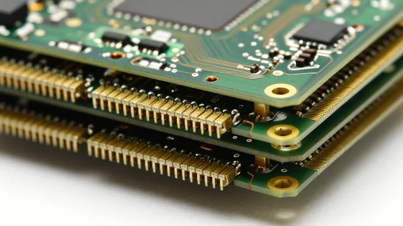
For sensitive In-Vitro Diagnostic (IVD) systems, PCB performance hinges on the manufacturer's ability to manage high-speed signals while minimizing dielectric loss and electromagnetic interference. Precision manufacturers must demonstrate mastery over high-frequency substrate selection and precise stack-up geometry to maintain the integrity of millivolt-level analog signals.
Material Performance Metrics for IVD Applications
| Material Property | Significance for IVD | Preferred Specification |
|---|---|---|
| Dissipation Factor (Df) | Reduces signal attenuation in high-speed data | < 0.005 @ 10GHz |
| Dielectric Constant (Dk) Stability | Ensures consistent impedance across the board | Tolerance < ±0.03 |
| Coefficient of Thermal Expansion | Prevents via barrel cracking during cycling | Matches Copper (approx 17 ppm/°C) |
Technical Competencies to Audit
- Controlled Impedance Verification
Does the manufacturer provide TDR (Time Domain Reflectometry) reports for every production panel to verify trace impedance stays within 5% of design targets? - Low-Loss Laminate Handling
Experienced partners should have validated workflows for processing advanced laminates like PTFE or ceramic-filled thermosets that require specific drilling and desmear parameters. - Stack-up Engineering Support
The partner must offer DFM (Design for Manufacturing) feedback to optimize layer counts and shielding, ensuring crosstalk is minimized between noisy digital sections and sensitive analog sensors.
Beyond technical capabilities, confirm that the manufacturer maintains a clean-room environment for high-layer-count builds to prevent microscopic contaminants from causing interlayer shorting or parasitic capacitance, both of which are catastrophic for sensitive IVD analytical instrumentation.
Manufacturing Precision: Cleanroom Capabilities and Cleanliness Standards
The Imperative of Controlled Manufacturing Environments
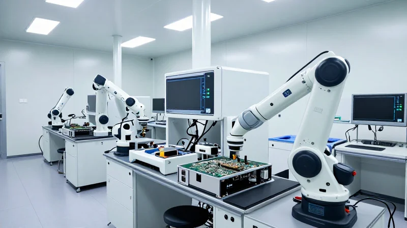
Sensitive In-Vitro Diagnostic (IVD) instrumentation operates on micro-volt level signals that are highly susceptible to interference caused by environmental particulates and ionic residues. High-precision PCB manufacturers must employ controlled environment protocols that go beyond standard assembly lines, utilizing certified ISO Class cleanrooms to mitigate the risk of dendritic growth and electrochemical migration that can cause catastrophic diagnostic failure.
Key Cleanliness Standards and Verification
Total cleanliness is not merely a visual assessment; it is a measurable technical requirement. Manufacturers must adhere to industry-recognized standards such as IPC-J-STD-001 and IPC-5704 to quantify ionic contamination. Failure to maintain these standards leads to leakage currents, which manifest as noise or drift in sensitive chemical sensing arrays.
| Contamination Type | Impact on IVD Hardware | Measurement Standard |
|---|---|---|
| Ionic Residues | Electrochemical migration and leakage current | IPC-J-STD-001 |
| Particulates | Impedance discontinuity in fine-pitch traces | ISO 14644-1 |
| Organic Contaminants | Degraded solder joint reliability | Ion Chromatography |
- Why is an ISO 14644-1 certification essential for my manufacturer?
This certification provides an objective baseline for cleanroom air quality, ensuring that the assembly environment is free from airborne contaminants that could adhere to PCB surfaces during the critical reflow process. - What is the danger of ionic contamination in IVD boards?
Ionic contamination, often left behind by flux residues, can react with humidity to form conductive pathways between traces. In precision diagnostics, these pathways create unpredictable micro-shorts that degrade signal-to-noise ratios. - How should a manufacturer prove their cleanliness levels?
A qualified partner should provide routine Ion Chromatography (IC) test reports and Surface Insulation Resistance (SIR) testing results to demonstrate that their cleaning processes consistently meet stringent medical-grade requirements.
DFM and Prototyping: Leveraging Early Engineering Collaboration
The Strategic Value of Early DFM Engagement
For sensitive In-Vitro Diagnostic (IVD) systems, PCB design choices made at the schematic level reverberate through manufacturing yield and instrument sensitivity. Engaging a manufacturing partner during the initial design phase allows for DFM (Design for Manufacturing) feedback that addresses potential bottlenecks—such as thermal management, trace geometry, and assembly tolerances—long before physical prototypes are fabricated. By leveraging the manufacturer's expertise early, engineering teams can proactively mitigate risks associated with signal interference and assembly yield, preventing expensive design spins that often plague sensitive medical diagnostic instrumentation.
DFM Impact on Prototype Efficacy
| Design Factor | Without DFM Input | With DFM Collaboration |
|---|---|---|
| Component Placement | Potential cross-talk/noise issues | Optimized for signal isolation |
| Layer Stack-up | Impedance mismatch in production | Balanced, EMI-resilient design |
| Pad/Trace Geometry | Solder bridging or weak joints | Yield-optimized assembly footprint |
Addressing Common Prototyping Questions
- How does early manufacturer involvement impact IVD instrument sensitivity?
Manufacturers can provide critical insights into layer stack-ups and material selection that reduce parasitic capacitance, directly improving the signal-to-noise ratio required for high-accuracy diagnostic measurements. - Why should I share design files before reaching the final prototype stage?
Sharing preliminary designs allows the manufacturer to flag manufacturing limitations, such as non-standard hole sizes or aspect ratios, that could otherwise hinder scaling to high-volume production later. - What documentation should I expect from a DFM-focused partner?
Expect formal DFM reports that identify non-conformances, recommendations for improved solder mask clearance, and insights into thermal dissipation paths for high-power diagnostic modules.
Ultimately, selecting a PCB manufacturer for IVD systems is not merely about procuring bare boards, but about establishing an engineering partnership. By integrating the manufacturer’s technical feedback into the prototype workflow, companies drastically reduce the 'time-to-market' while ensuring the final diagnostic system meets the stringent precision requirements of clinical healthcare environments.
Testing Protocols: Beyond Basic Visual Inspection
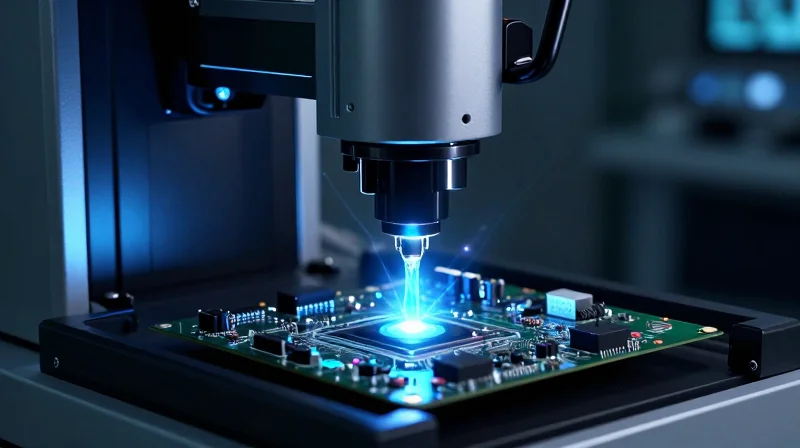
For sensitive In-Vitro Diagnostic (IVD) instrumentation, standard visual inspections are insufficient to catch latent defects that can compromise diagnostic accuracy. High-precision PCB manufacturing requires multi-layered testing regimes that leverage automated, non-destructive methodologies to verify internal structural integrity, component placement, and electrical performance at a microscopic level.
Advanced Automated Verification Technologies
| Inspection Method | Primary Application | Advantage for IVD Systems |
|---|---|---|
| Automated Optical Inspection (AOI) | Surface mount components and solder joints | High-speed detection of missing components or polarity errors. |
| Automated X-ray Inspection (AXI) | BGA, CSP, and multi-layer internal layers | Visualizes solder voids and hidden connections under chips. |
| Flying Probe Testing | Bare board and populated assembly connectivity | Ideal for prototyping and high-mix, low-volume medical runs. |
The Role of X-ray Inspection in Multi-Layer Reliability
Complex IVD instrumentation often utilizes dense multi-layer boards. Automated X-ray Inspection (AXI) is non-negotiable for these designs. By penetrating the board to identify internal solder bridges, insufficient solder wetting, or internal layer registration offsets, AXI provides a level of quality assurance that physical probing cannot reach, directly preventing failures in high-precision sensing circuits.
Common Questions on Testing Protocols
- Why is Flying Probe preferred over Bed-of-Nails for medical prototypes?
Flying probe testing offers superior flexibility for design iterations by eliminating the need for expensive, custom test fixtures, allowing for rapid updates to test programs as engineering evolves. - How does AOI mitigate risks in sensitive IVD diagnostics?
AOI ensures strict adherence to component placement and solder meniscus geometry, preventing intermittent electrical connections that could cause signal noise or false readings in sensitive diagnostic measurements. - What frequency should testing be conducted?
For medical-grade production, 100% inspection through both AOI and AXI is recommended at every critical process gate to maintain the rigorous quality standards required for regulatory compliance.
Supply Chain Transparency and Long-Term Component Traceability
Ensuring Integrity in the IVD Component Supply Chain
For sensitive In-Vitro Diagnostic (IVD) instrumentation, the integrity of every component—from high-precision resistors to specialized ICs—is non-negotiable. A top-tier PCB manufacturer must provide full supply chain visibility, ensuring that every batch of material is authenticated and tracked to its original point of manufacture. This rigor is the only reliable defense against counterfeit parts, which pose catastrophic risks to diagnostic accuracy and patient safety.
Mitigating Obsolescence and Counterfeit Risks
- How does verified sourcing prevent counterfeit integration?
Reputable manufacturers mandate strict adherence to AS6081/AS6171 standards, sourcing exclusively from authorized distributors or direct from the OEM, maintaining a documented chain of custody for every serialized component. - What is the strategy for long-term obsolescence management?
Proactive lifecycle monitoring, utilizing platforms like SiliconExpert or IHS Markit, allows manufacturers to identify end-of-life (EOL) components early, enabling last-time buy (LTB) coordination or engineering redesigns before supply halts.
Traceability Standards Comparison
| Feature | Baseline Capability | High-Precision Medical Standard |
|---|---|---|
| Component Sourcing | Open Market/Distributors | Authorized/Tier-1 OEMs Only |
| Traceability Depth | Lot Code Level | Individual Serial Number/Date Code |
| Obsolescence Monitoring | Reactive/Ad-hoc | Automated Lifecycle Analytics |
| Counterfeit Testing | Visual Only | Destructive/Non-Destructive Testing |
By demanding full traceability, your organization ensures that every medical device manufactured under your brand meets the stringent quality requirements mandated by the FDA and international regulatory bodies like the MDR. Partnering with a PCB manufacturer that prioritizes supply chain hygiene is an investment in the long-term viability and reliability of your diagnostic instrumentation.
The Final Vetting: Conducting an Effective On-Site Audit
The Anatomy of a Technical On-Site Audit
When auditing a PCB fabrication facility for high-precision IVD instrumentation, your focus must shift from corporate sales presentations to empirical observation of the shop floor. You are verifying that the manufacturer's stated capabilities match their actual environmental controls, equipment calibration status, and operator adherence to cleanroom standards.
| Audit Focus Area | Key Metric to Observe | Significance for IVD |
|---|---|---|
| Environmental Controls | Cleanroom particle count / Humidity logs | Prevents microscopic debris that could cause signal interference. |
| Equipment Maintenance | Calibration sticker currency on SPI/AOI units | Ensures measurement repeatability for tight-tolerance boards. |
| ESD Management | Wrist strap testing and floor grounding | Protects sensitive CMOS and diagnostic ICs from latent failures. |
| Process Flow | In-process WIP tagging and FIFO implementation | Prevents contamination and minimizes board handling risk. |
Critical Questions for the Production Leadership
- How do you handle 'scrap-on-defect' versus rework?
For IVD applications, rework often introduces risks of delamination or intermetallic issues; a robust manufacturer should have a documented policy limiting rework on high-layer-count sensitive boards. - Can you demonstrate the real-time traceability of a board from start to finish?
Ask them to trace one random serial number back to the raw laminate and chemical bath logs to verify the integrity of their ERP system. - How is the change management process documented for technical modifications?
Verify that any deviation from the original Gerber-validated process triggers an Engineering Change Order (ECO) that you are required to approve before production continues.
Validation of Human Performance
Beyond machinery, observe the training and behavior of the personnel. In high-precision manufacturing, the 'culture of quality' is often visible in how technicians handle the boards—using proper PPE, following structured work instructions at every station, and immediately flagging anomalies. If you witness deviations from these standard operating procedures without explanation, it is a primary indicator of a fragile manufacturing process that will likely result in inconsistent quality during mass production of your IVD hardware.
Selecting a PCB manufacturing partner for IVD instrumentation is a high-stakes decision that demands due diligence across regulatory, technical, and operational dimensions. By prioritizing ISO 13485 standards, signal integrity expertise, and advanced inspection capabilities, you secure the reliability of your diagnostic platforms. Ready to take the next step in your procurement strategy? Contact our engineering team today to discuss your project requirements and learn how we support high-precision medical innovation.
