
In the race to develop increasingly portable yet powerful aesthetic medical devices, the traditional silicon-based power architecture has hit a thermal and physical ceiling. As devices shrink, the demand for higher energy efficiency and compact power delivery becomes critical. This article examines the technological shift toward Gallium Nitride (GaN) and what it means for the next generation of aesthetic laser PCBs.
The Evolution of Power Electronics in Aesthetic Medicine
From Industrial Footprints to Clinical Versatility
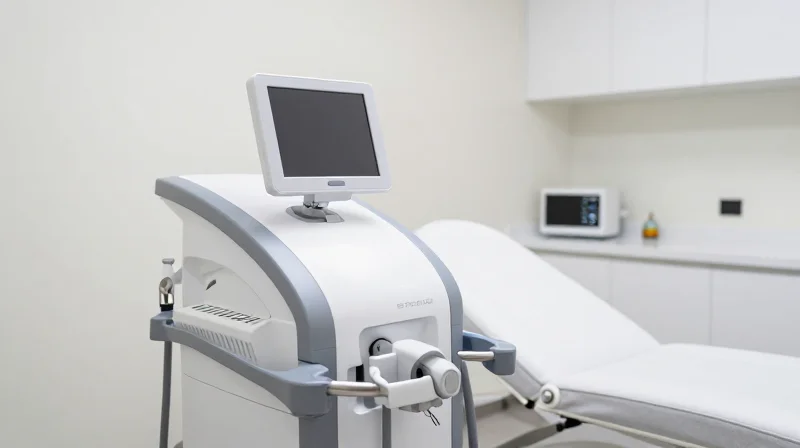
Historically, aesthetic laser systems were defined by their cumbersome size, often occupying significant floor space in medical spas and dermatology clinics. These legacy systems relied heavily on traditional Silicon (Si) MOSFET technology, which required extensive cooling infrastructure and bulky power conversion circuits to manage thermal output and electrical switching demands. As the industry has pushed for high-repetition rates and higher peak powers, the physical limitations of Silicon have dictated the structural constraints of laser platforms.
The Role of Wide-Bandgap Semiconductors
The recent integration of Gallium Nitride (GaN) into Power PCBS has shattered these traditional constraints. GaN semiconductors possess superior electron mobility and higher breakdown voltages compared to Silicon. By operating at higher switching frequencies, GaN allows for the miniaturization of inductive and capacitive components. This reduction in power stage volume directly correlates to the emergence of high-performance handheld devices that maintain the same energy density as their stationary predecessors.
| Feature | Legacy Silicon (Si) MOSFETs | Gallium Nitride (GaN) FETs |
|---|---|---|
| Switching Speed | Limited/Slow | Ultra-Fast |
| Thermal Efficiency | Moderate (High Heat Loss) | High (Lower Losses) |
| Form Factor | Bulky/Floor Units | Compact/Portable |
| Power Density | Standard | Exceptional |
Frequently Asked Questions
- Why was Silicon the industry standard for so long?
Silicon was favored for its low production costs, established manufacturing ecosystem, and sufficient performance for lower-frequency laser applications. - Does GaN technology affect treatment outcomes?
Yes, by allowing for faster pulse-width modulation and more stable power delivery, GaN-based systems offer improved pulse precision, resulting in better clinical efficacy and safer energy delivery. - What is the primary barrier to GaN adoption?
While GaN provides superior technical performance, the primary barrier has historically been the higher component cost and the complexity of integrating high-frequency gate drivers into existing PCB designs.
The Limitations of Legacy Silicon MOSFETs
The Silicon Ceiling: Why MOSFETs Are Reaching Their Limits
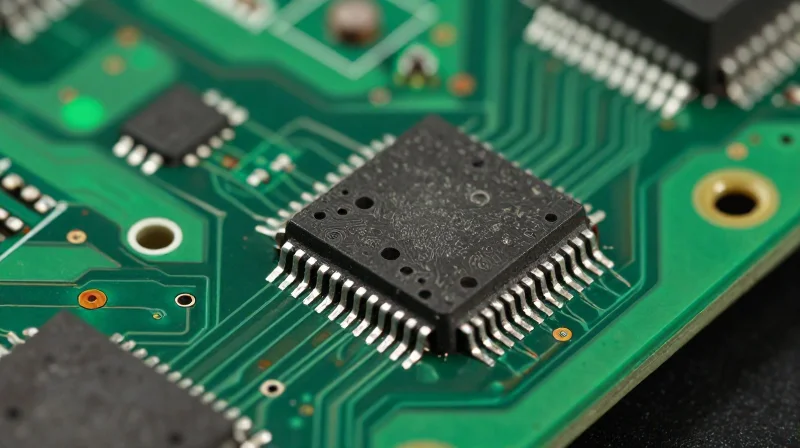
As aesthetic laser applications demand higher pulse frequencies and increased energy output, silicon (Si) MOSFETs are increasingly viewed as a technological bottleneck. Silicon has served as the industry standard for decades, but it is now constrained by fundamental material physics—specifically its relatively low bandgap energy. This limitation forces designers to choose between bulky thermal management systems and diminished power efficiency.
Critical Performance Bottlenecks
- Switching Loss and Frequency
Silicon MOSFETs suffer from high gate charge and parasitic capacitances, leading to significant switching losses at high frequencies. This limits the pulse control precision essential for modern aesthetic procedures. - Thermal Management Requirements
Due to higher on-resistance (RDS(on)) at elevated temperatures, Si components require oversized heat sinks and active cooling fans, which directly conflict with the trend toward miniaturized, portable laser devices. - Footprint and Power Density
The inability to operate efficiently at high frequencies forces power converters to rely on larger passive components like inductors and capacitors, resulting in a larger PCB footprint.
| Parameter | Silicon MOSFET Limitation | Resulting Design Constraint |
|---|---|---|
| Switching Speed | Low/Moderate | Larger passive components |
| Thermal Conductivity | Moderate | Bulky heat sinking |
| Breakdown Voltage | Limited | Complex multi-stage circuits |
To achieve the next level of precision in aesthetic lasers—such as ultra-short picosecond pulses—engineers must bypass these silicon limitations. The inherent resistance and thermal degradation of silicon under high-current, high-frequency operation create a ceiling that prevents further shrinking of power delivery modules, ultimately dictating the bulkiness of current-generation aesthetic platforms.
Enter Gallium Nitride (GaN): A Paradigm Shift in Power Density

The Material Advantage of Wide-Bandgap Semiconductors
Gallium Nitride (GaN) represents a fundamental departure from traditional Silicon-based power electronics. By utilizing a wide-bandgap (WBG) material structure, GaN devices can withstand higher voltages and operate at significantly higher temperatures than silicon, effectively eliminating the primary thermal bottlenecks that have historically limited aesthetic laser portability.
Key Performance Metrics: GaN vs. Silicon
| Feature | Silicon (Si) MOSFET | Gallium Nitride (GaN) |
|---|---|---|
| Bandgap Energy | 1.1 eV | 3.4 eV |
| Electron Mobility | Moderate | Extremely High |
| Switching Speed | KHz Range | MHz Range |
| Thermal Conductivity | Standard | Superior |
Technical Benefits for Aesthetic Lasers
The higher electron mobility of GaN allows for much faster switching frequencies compared to silicon. In practical terms, this means that the passive components within a laser’s power supply—such as inductors and capacitors—can be dramatically reduced in size. This reduction allows manufacturers to shrink the overall chassis of aesthetic laser devices without sacrificing the high peak power required for effective skin resurfacing or hair removal treatments.
- How does GaN reduce device footprint?
Faster switching speeds allow for smaller reactive components (inductors and transformers), leading to a more compact Power PCB design. - Why is thermal management easier with GaN?
GaN devices exhibit lower switching and conduction losses, generating less waste heat and reducing the reliance on bulky internal cooling systems. - Does GaN affect treatment quality?
Yes, superior power control enables tighter pulse precision and more stable energy delivery, which are critical for predictable clinical outcomes in aesthetic procedures.
Comparing Switching Speeds and Efficiency
Overcoming the Switching Speed Barrier
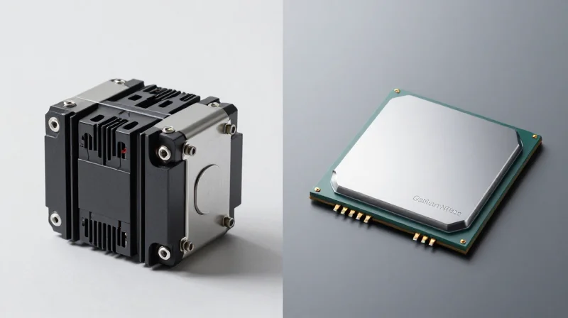
The primary advantage of GaN over traditional Silicon (Si) MOSFETs lies in its superior electron mobility, which allows for vastly higher switching frequencies. In legacy silicon systems, designers are often forced to choose between lower frequencies—to avoid excessive heat buildup—and larger passive components. GaN eliminates this trade-off. By operating at MHz-range frequencies, GaN allows power supply designers to utilize significantly smaller inductors and capacitors, directly contributing to the miniaturization of handheld aesthetic laser devices.
Efficiency and Thermal Management Comparison
| Parameter | Silicon MOSFET | Gallium Nitride (GaN) |
|---|---|---|
| Switching Speed | Moderate (kHz range) | Ultra-fast (MHz range) |
| Thermal Efficiency | Higher conduction loss | Superior thermal performance |
| Passive Components | Bulky/Large | Compact/Small |
| Energy Dissipation | Higher waste heat | Minimal switching losses |
Impact on PCB Design
Transitioning to GaN technology allows engineers to achieve a higher power density, meaning more energy is delivered to the laser diodes with fewer conversion losses. Because GaN switches exhibit minimal parasitic capacitance, the energy wasted during each switching event is reduced by up to 70% compared to silicon. This efficiency gain translates into a reduced requirement for bulky heat sinks and complex cooling fans, allowing for sleeker, more ergonomic laser handpieces that remain cool to the touch during extended clinical use.
Technical FAQ
- Why does faster switching decrease component size?
Higher frequencies allow the energy storage requirements of passive components like inductors and transformers to decrease proportionally, enabling the use of much smaller surface-mount parts. - How does GaN handle thermal management differently?
GaN provides lower gate charge and output capacitance, resulting in drastically lower switching losses which generate less ambient heat within the power PCB. - Is the transition from Si to GaN complex?
While GaN requires specific gate drive designs to manage its high-speed signals, the reduction in overall system complexity and the removal of secondary cooling stages often yield a net benefit in design simplicity.
Impact on PCB Layout and Thermal Management
Miniaturization and Footprint Efficiency
The primary advantage of GaN in aesthetic laser hardware lies in its ability to operate at significantly higher switching frequencies. Because GaN-based power stages require much smaller energy storage components—specifically inductors and capacitors—engineers can drastically shrink the power delivery board. This enables manufacturers to shift from bulky, cabinet-sized aesthetic systems to portable, ergonomic handheld devices without sacrificing peak power output.
Thermal Management and PCB Design
GaN MOSFETs minimize heat dissipation at the source due to lower on-resistance and significantly lower switching losses. This efficiency shift allows for more aggressive PCB layouts, where components can be packed more densely without risking thermal runaway or performance degradation.
| Parameter | Silicon MOSFET Impact | GaN FET Impact |
|---|---|---|
| Passive Component Size | Large (due to low frequency) | Small (due to high frequency) |
| Heat Sink Mass | High (Active cooling required) | Low (Passive or minimal cooling) |
| Board Density | Limited by thermal spacing | High density permitted |
Frequently Asked Questions
- Does GaN allow for the total removal of heat sinks?
While GaN operates much cooler, it rarely allows for total removal of cooling solutions. However, it permits a reduction in heat sink volume by up to 50-70%, allowing for smaller, lighter enclosures. - How does GaN affect PCB trace routing?
Because GaN switches much faster, layout becomes more sensitive to parasitic inductance. Engineers must adopt shorter, more direct routing strategies to avoid EMI and voltage ringing. - Is the transition to GaN cost-effective for PCB manufacturing?
While individual GaN components are more expensive, the total system cost often drops due to lower requirements for expensive copper cooling, aluminum heat sinks, and overall chassis material.
Reliability and Cost Considerations for Medical Equipment
Reliability Metrics in Clinical Environments
While Silicon MOSFETs have a decades-long track record of reliability, Gallium Nitride (GaN) has moved beyond experimental status to meet rigorous industrial standards, such as JEDEC qualification. In clinical aesthetic laser applications, the reliability concern often centers on dynamic on-resistance (RDS(on))—a phenomenon where the device resistance increases during high-voltage stress. Modern GaN-on-Si platforms have mitigated this effectively, proving their resilience in environments requiring millions of switching cycles without significant degradation.
| Feature | Silicon MOSFET | GaN Power FET |
|---|---|---|
| Maturity | High (Proven) | Evolving (High-Reliability) |
| Failure Mode | Thermal Runaway | Dynamic RDS(on) (Managed) |
| Gate Sensitivity | Robust | Requires Precision Drive |
| MTBF (Expected) | Very High | Comparable in Targeted Apps |
Total Cost of Ownership and Economic Factors
The price point of GaN components is inherently higher than mature silicon MOSFETs on a unit-cost basis. However, system-level cost analysis suggests that GaN can be more cost-effective due to reduced board space requirements, smaller heat sinks, and fewer passive components. Aesthetic laser manufacturers can leverage these savings to reduce the overall Bill of Materials (BOM) and achieve higher power density in smaller, more portable devices.
Frequently Asked Questions
- Is GaN technology reliable enough for 24/7 clinical use?
Yes, when correctly implemented with gate drivers tuned for high switching speeds, GaN devices exceed the reliability benchmarks required for continuous operation in medical aesthetic platforms. - Does the higher component cost offset total savings?
Usually not. Savings from heat sink reduction, smaller footprint, and increased efficiency often result in a lower total system cost compared to legacy silicon-based designs. - What is the primary risk factor with GaN adoption?
The primary challenge is the requirement for specialized layout design and precise gate driving to manage high dV/dt rates and prevent potential signal integrity issues.
Future-Proofing Aesthetic Laser Systems
Strategic Roadmap for GaN Implementation
Engineering teams must move beyond simple component swapping to fully realize the benefits of GaN technology. Future-proofing aesthetic lasers necessitates a fundamental redesign of power delivery networks (PDNs) that accounts for the ultra-fast switching characteristics of wide-bandgap devices, which traditional silicon-based architectures cannot effectively accommodate.
| Strategy | Legacy Silicon Approach | Future-Proof GaN Approach |
|---|---|---|
| Board Density | Component-heavy, larger footprints | Miniaturization through higher switching frequencies |
| EMI Mitigation | Standard RC filtering | Integrated layout-level impedance control |
| Thermal Strategy | Active forced air cooling | Advanced PCB material utilization (IMS/Ceramic) |
Addressing Design Challenges
Transitioning to GaN is not without engineering friction. The primary challenge remains parasitic inductance, which can trigger voltage ringing in high-speed switching loops. Teams should prioritize layout optimization, minimizing trace lengths and employing low-inductance package designs to maintain device integrity and signal quality.
- How does GaN adoption affect long-term maintenance?
By reducing thermal stress on surrounding PCB components through higher efficiency, GaN significantly extends the mean time between failures (MTBF) for high-power laser systems. - Is GaN economically viable for mid-range lasers?
While component costs are higher than silicon, the total system cost is often reduced due to the elimination of heavy heat sinks, smaller passive components, and decreased power supply unit (PSU) volume. - What should be the first step in the transition?
Start with modular power stage replacements to validate efficiency gains in existing cooling architectures before migrating to full-scale board miniaturization.
/* Design Rule Check (DRC) adjustment for GaN */
const MAX_PARASITIC_INDUCTANCE = '0.5nH';
const GATE_LOOP_LENGTH = 'minimize';
const BYPASS_CAPACITOR_PLACEMENT = 'immediate_vicinity_of_drain';
// Ensure return path is directly beneath signal trace to optimize loop area.
The transition to GaN technology is no longer a futuristic concept but a necessary evolution for companies aiming to lead the aesthetic medical market. By embracing higher power density and improved thermal efficiency, manufacturers can deliver more effective, portable, and reliable laser systems. Are you ready to optimize your device's power architecture? Contact our engineering consultancy team today to discuss your next-generation PCB design requirements.
