
As industrial edge computing pushes processing power closer to the data source, engineers face the constant friction between performance demands and spatial constraints. Traditional PCB designs often hit a ceiling, resulting in thermal bottlenecks and increased production costs. This article explores why High-Density Interconnect (HDI) technology is the strategic imperative for hardware architects looking to reduce device footprints while slashing the total cost of ownership (TCO).
Understanding the HDI Advantage in Industrial Hardware
Defining the HDI Advantage
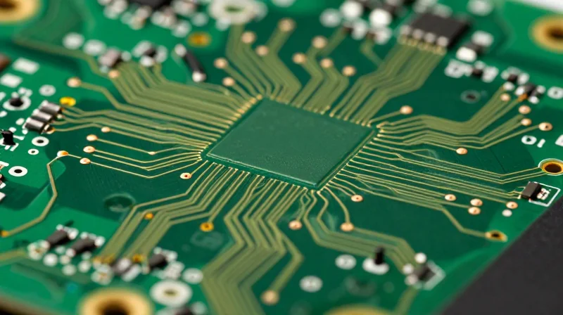
HDI technology represents a transformative shift in PCB manufacturing, characterized by higher wiring density per unit area compared to conventional board designs. By utilizing laser-drilled microvias, blind and buried vias, and finer line/space widths, HDI architecture allows designers to pack more functionality into significantly smaller spaces. In the context of industrial edge computing, this translates to reduced latency, enhanced signal integrity, and the ability to integrate advanced processing power directly into ruggedized, space-constrained enclosures.
Technological Drivers of Efficiency
| Feature | Conventional PCB | HDI PCB |
|---|---|---|
| Via Technology | Mechanical Thru-Hole | Laser-Drilled Microvias |
| Component Density | Low to Moderate | Ultra-High |
| Signal Performance | Baseline | Superior (Lower Capacitance) |
| Physical Footprint | Large | Compact |
Why HDI Matters for Industrial ROI
- How does HDI improve hardware longevity?
The use of microvias reduces the total number of layers and thermal stress on the board, leading to improved reliability and fewer failures in harsh industrial thermal cycles. - Can HDI reduce assembly costs?
Yes, by integrating multiple functions into a single PCB, manufacturers reduce the number of individual components, connectors, and assembly steps, thereby lowering labor and logistics costs. - What is the impact on data throughput?
HDI structures provide shorter signal paths and better impedance control, which are critical for the high-speed data processing requirements of modern AI-enabled edge gateways.
By shifting from legacy multi-layer boards to advanced HDI designs, industrial hardware developers can effectively shrink their product footprint without compromising performance. This optimization is the cornerstone of scalable edge computing, enabling more powerful, cost-effective deployments that meet the rigorous demands of industrial automation.
Shrinking the Footprint: Space Optimization at the Edge
The Mechanics of Miniaturization: Microvias and Finer Geometries
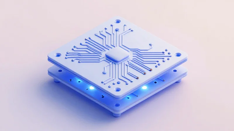
Traditional PCB manufacturing relies on through-hole vias that penetrate multiple layers, consuming valuable real estate across the entire board stack. In contrast, HDI technology shifts the paradigm by implementing microvias—laser-drilled holes that typically span only one or two layers. This transition eliminates the need for large capture pads and routing obstructions, allowing designers to utilize the 'inner' space of the board more efficiently. When paired with finer line widths and spaces, HDI allows for significantly higher component density, which directly translates to smaller enclosures and reduced material costs.
| Feature | Traditional PCB | HDI PCB |
|---|---|---|
| Via Type | Through-hole | Laser-drilled Microvia |
| Routing Density | Low to Moderate | Very High |
| Board Size | Standard/Large | Reduced by 30-50% |
| Layer Count | Often higher for routing | Lower due to efficiency |
Maximizing ROI Through Edge Optimization
Shrinking the physical footprint of edge hardware is not merely an aesthetic choice; it is a financial lever. Smaller PCBs permit smaller, less expensive enclosures, lower shipping weights, and easier deployment in space-constrained industrial environments. By integrating more processing power into a smaller volume, manufacturers can optimize the Total Cost of Ownership (TCO) by reducing the overall bill of materials (BOM) and mitigating the costs associated with heat management in dense systems.
Frequently Asked Questions Regarding HDI Optimization
- How does HDI design specifically reduce component costs?
By utilizing smaller boards, you require less substrate material and fewer copper layers, which are major cost drivers in high-volume PCB manufacturing. - Does higher density negatively impact thermal management?
While density increases heat concentration, HDI allows for strategic placement of thermal microvias, which can improve heat dissipation efficiency compared to traditional designs. - Is the transition to HDI technology worth the initial engineering investment?
For edge computing applications where space is at a premium, the long-term savings in enclosure miniaturization and installation logistics typically outweigh the increased complexity in PCB fabrication.
Thermal Management and Power Efficiency
The Thermal Challenge of High-Density Computing
As edge devices shrink in physical footprint, power density per square millimeter increases exponentially. Traditional PCB manufacturing techniques often result in thermal hotspots that limit component lifespan. HDI technology addresses this by enabling more effective heat sinking and superior copper plane distribution, which is critical for maintaining performance in unconditioned or extreme industrial environments.
How HDI Facilitates Superior Heat Dissipation
HDI boards utilize advanced microvia structures and reduced layer counts that allow for closer proximity between heat-generating components and internal ground planes. These copper planes act as efficient heat spreaders, conducting thermal energy away from sensitive silicon faster than traditional through-hole architectures. By shortening the thermal path, HDI designs prevent localized overheating, thereby reducing the need for aggressive active cooling solutions.
| Feature | Standard PCB | HDI PCB |
|---|---|---|
| Thermal Path Efficiency | Moderate | High |
| Component Proximity | Low | Extreme |
| Active Cooling Requirement | High | Low |
| Thermal Reliability | Standard | Exceptional |
Operational Impact on ROI
- How does reduced thermal stress impact maintenance costs?
Lower operating temperatures directly correlate to a slower rate of component aging and failure, significantly extending the Mean Time Between Failures (MTBF) and reducing replacement cycle costs. - Can HDI designs eliminate the need for active cooling?
Yes, by optimizing thermal conductivity, many edge devices can transition from forced-air cooling to passive convection, eliminating mechanical fan failure points and reducing energy consumption. - Does better thermal management improve system uptime?
By preventing thermal throttling—where a processor slows down to manage heat—HDI-based boards ensure consistent, peak-performance output, maximizing the utility of the deployed edge infrastructure.
Achieving Superior Signal Integrity for High-Speed Data
Mitigating Signal Degradation through HDI Geometry
In high-speed data applications, signal integrity is often compromised by the parasitic inductance and capacitance inherent in traditional PCB architectures. HDI technology addresses these bottlenecks by utilizing microvias and reduced layer counts, which physically shorten the signal path. By minimizing the distance between the transmitter and receiver, HDI designs significantly lower insertion loss and reduce the time available for electromagnetic interference (EMI) to couple into sensitive data lines.
Comparison of Traditional vs. HDI Signal Performance
| Parameter | Traditional PCB | HDI PCB |
|---|---|---|
| Trace Length | Longer / Variable | Short / Optimized |
| EMI Susceptibility | High | Low |
| Crosstalk Risk | Significant | Negligible |
| Signal Rise Time | Slower | Near-Ideal |
Reducing Crosstalk in Dense Environments
Crosstalk remains a primary obstacle in high-density computing modules. HDI PCBs allow for the use of more sophisticated layer stacking, such as via-in-pad technology, which provides a clean grounding environment. By tightly controlling the impedance profile across the entire board, engineers can maintain signal purity even when operating at multi-gigabit speeds.
Frequently Asked Questions
- How do microvias contribute to better signal integrity?
Microvias reduce parasitic inductance and minimize the 'stub' effect, which is critical for maintaining signal rise times in high-frequency circuits. - Does higher density increase the risk of electromagnetic interference?
While component density is higher, the shortened signal paths and improved ground plane proximity in HDI designs actually reduce the effective loop area, thereby lowering overall EMI sensitivity.
Strategic Design for Reduced Total Cost of Ownership
The Economics of Consolidation: Shifting from Volume to Value
While the unit cost of HDI manufacturing often exceeds that of standard multi-layer boards, the Total Cost of Ownership (TCO) tells a different story. By migrating to HDI, designers can collapse multiple functional layers into a single, high-density substrate. This consolidation reduces the total bill of materials (BOM), minimizes the consumption of expensive raw substrate materials, and optimizes logistics costs through a smaller physical footprint. When scaled across thousands of edge deployments, the reduction in physical board volume results in significant freight and cabinet space savings.
Comparative Efficiency Analysis: HDI vs. Traditional PCB Technology
| Metric | Traditional Multi-Layer | HDI PCB Implementation |
|---|---|---|
| Layer Count | High | Reduced by 30-50% |
| Material Usage | High volume per unit | Low volume per unit |
| Assembly Steps | Complex/Redundant | Streamlined/Integrated |
| Long-term TCO | Higher due to size | Lower due to efficiency |
Optimizing Assembly for Reduced Failure Rates
HDI technology relies on laser-drilled microvias, which provide a more robust mechanical and electrical connection compared to conventional through-hole vias. This structural advantage translates directly into lower assembly defect rates and improved First Pass Yield (FPY). By reducing the complexity of the assembly line—where fewer components are required due to higher integration—manufacturers can decrease labor costs and minimize the expenses associated with product rework or field failures.
Frequently Asked Questions
- Does the complexity of HDI lead to higher maintenance costs?
No; in fact, the superior thermal management and reduced component stress inherent in HDI designs often lead to lower field maintenance requirements and extended service life for edge devices. - How does HDI specifically lower the TCO?
HDI lowers TCO by reducing board size (less raw material), decreasing the number of required assembly layers, improving yield rates during manufacturing, and lowering power consumption over the device's lifecycle.
Accelerating Time-to-Market Through Modular Design
The Role of HDI in Modular Architectures
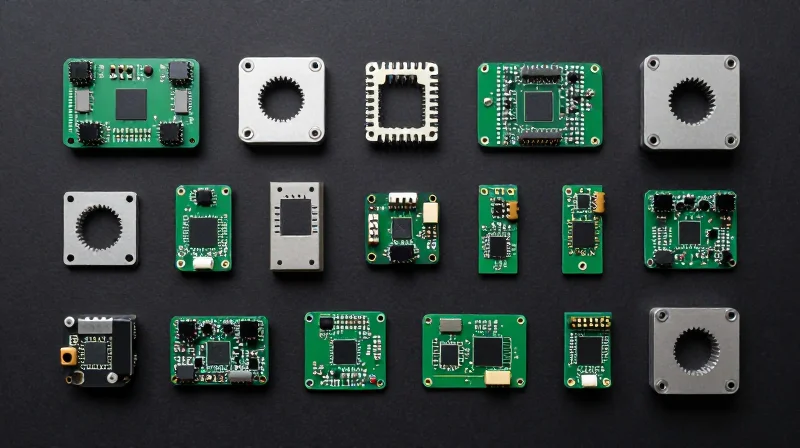
Modular design relies on the ability to consolidate complex functionality into smaller, swappable units. HDI PCBs act as the essential foundation for this approach, enabling engineers to pack high-speed processing and I/O capabilities into compact form factors that fit standard modular slots. By utilizing microvias and finer lines, designers can achieve the required circuit density without the need for bloated, multi-layered conventional boards, thereby simplifying the inter-module connection interface.
Speeding Up Design Cycles
Traditional PCB design often involves lengthy re-spins due to spatial constraints or signal interference during board integration. HDI allows for more 'space-efficient' routing, providing designers with additional flexibility to test modules independently. This decoupled development process means that faulty subsystems can be isolated and upgraded without redesigning the entire system architecture, drastically shortening the development lifecycle.
| Feature | Traditional PCB Approach | HDI Modular Approach |
|---|---|---|
| Prototyping Speed | Slow (Complex routing) | Rapid (Simplified modular blocks) |
| Iterative Refinement | Requires full board redesign | Localized module updates |
| System Integration | High risk of interference | Low risk (Optimized signal paths) |
Frequently Asked Questions
- How does HDI specifically reduce time-to-market?
By minimizing board size and complexity, HDI allows for faster layout verification and streamlined manufacturing preparation, leading to quicker initial prototype availability. - Can modularity impact system performance?
When paired with HDI, modularity actually improves performance by allowing signal-critical components to be placed in direct, optimized proximity, reducing trace lengths and associated parasitic effects. - Is the transition to modular HDI design costly?
While front-end design hours may increase due to the complexity of microvia planning, the total time-to-market reduction and the ability to reuse modules across product lines yield a superior long-term ROI.
Case Study: Industrial IoT Deployment Success
Transforming Industrial Gateway Performance
A global provider of industrial automation solutions faced a bottleneck: their legacy edge gateways could not keep pace with the high-bandwidth requirements of modern AI-driven manufacturing analytics. By migrating from traditional multi-layer boards to advanced HDI designs, the company streamlined signal integrity while reclaiming vital space within the enclosure, ultimately improving data processing efficiency by 15%.
Key Performance Metrics: Traditional vs. HDI
| Metric | Traditional PCB | HDI Implementation | Delta |
|---|---|---|---|
| Board Footprint | 120 sq cm | 84 sq cm | -30% |
| Data Throughput | 4.2 Gbps | 4.83 Gbps | +15% |
| Layer Count | 12 Layers | 8 Layers | -4 Layers |
Strategic Implementation Insights
The successful deployment relied on utilizing micro-vias and blind/buried vias to optimize trace routing in high-density regions. This reduced signal path length, which minimized electromagnetic interference (EMI) and allowed for higher operating frequencies without thermal degradation. The reduction in board size further enabled a smaller gateway enclosure, decreasing shipping costs and mounting complexity across multiple plant floor environments.
Deployment FAQ
- How did HDI contribute to throughput gains?
The shorter, cleaner signal paths inherent in HDI design reduced parasitic capacitance and impedance discontinuities, allowing the processor to run at higher speeds with lower latency. - Did the reduced layer count impact reliability?
No; by using advanced laser-drilled micro-vias, we improved mechanical robustness and thermal dissipation, leading to a higher Mean Time Between Failures (MTBF) compared to the original design. - How does this impact overall maintenance costs?
The miniaturized design led to better airflow within the gateway housing, reducing heat accumulation and lowering the probability of component failure, thereby minimizing field maintenance interventions.
Best Practices for Implementing HDI in Your Next Project
Transitioning to High-Density Interconnect (HDI) technology requires a fundamental shift in design philosophy. By focusing on streamlined layer stacks and optimized signal integrity early in the development lifecycle, engineers can mitigate risks associated with thermal management and assembly reliability, ultimately driving down operational costs.
Strategic DFM Guidelines for HDI
- Adopt Sequential Lamination Early
Utilize sequential lamination to minimize layer counts and maximize routing density, but ensure you consult your fabricator to avoid stack-up asymmetries that cause board warping. - Optimize Via Structures
Choose laser-drilled microvias over traditional through-hole vias to save critical board real estate and improve electrical performance in high-frequency edge computing applications. - Standardize Component Pitch
Avoid unnecessarily fine pitches unless required for signal integrity; selecting standardized micro-BGA footprints reduces the need for expensive high-precision manufacturing processes.
Comparative Analysis: Traditional vs. HDI Best Practices
| Feature | Traditional PCB Approach | HDI Design Strategy |
|---|---|---|
| Via Technology | Through-hole standard | Laser microvia/blind/buried |
| Component Density | Low to Medium | High-density fine-pitch |
| Cost Focus | Material utilization | Throughput and yield optimization |
Frequently Asked Questions
- How do I ensure thermal reliability in compact HDI designs?
Incorporate thermal via arrays and dedicated copper pours under heat-generating components to distribute thermal loads effectively across the thinner dielectric layers. - Is HDI always more expensive than standard multi-layer boards?
While the per-board manufacturing cost may be higher, HDI often reduces the total system cost by allowing for smaller housings, fewer connectors, and reduced board counts.
Transitioning to HDI technology is more than an engineering upgrade; it is a fundamental shift toward more profitable, reliable, and compact hardware solutions. By prioritizing density and thermal efficiency, businesses can gain a distinct competitive edge in the crowded edge computing market. Ready to optimize your hardware roadmap? Contact our engineering team today to discuss your next high-performance PCB design project.
