
In the hyper-competitive world of Industrial IoT, the true cost of a device is rarely found on the initial invoice. For engineering managers, the 'hidden tax' of sub-par PCB assembly manifests in premature field failures and escalating maintenance cycles. By prioritizing precision manufacturing today, you secure operational longevity that transforms your balance sheet tomorrow.
The Hidden Costs of 'Good Enough' Manufacturing
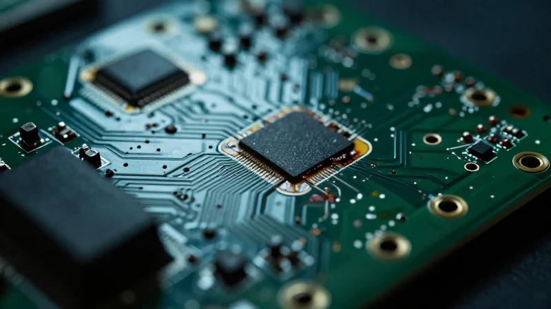
The False Economy of Minimum Specifications
Organizations often prioritize lower upfront unit costs, failing to account for the Total Cost of Ownership (TCO) associated with suboptimal hardware. When PCB manufacturing processes prioritize speed or low-cost materials over reliability, the resulting vulnerabilities—such as poor solder joint integrity and inferior thermal management—become recurring liabilities that manifest as field failures, requiring costly maintenance cycles.
Common Manufacturing Failure Drivers
| Failure Driver | Immediate Impact | Long-term Maintenance Cost |
|---|---|---|
| Substandard Solder | Micro-fractures and brittle joints | High field service labor costs |
| Inadequate Thermal Relief | Component degradation | Accelerated device replacement cycles |
| Grey Market Sourcing | Inconsistent performance | Reactive emergency troubleshooting |
Strategic Implications for Industrial IoT
In remote or mission-critical industrial environments, the cost of a single technician site visit often exceeds the total savings gained during the initial procurement phase. Optimized manufacturing—defined by rigorous Design for Manufacturing (DFM) checks, certified component supply chains, and automated optical inspection (AOI)—is not an overhead expense; it is a critical investment in operational continuity.
- How does PCB quality impact IoT maintenance?
High-quality manufacturing reduces the probability of environmental failure (vibration/heat), significantly lowering the frequency of required onsite technical interventions. - What is the primary risk of using low-cost components?
Component inconsistency leads to unpredictable system drift and shorter mean time between failures (MTBF), forcing expensive, unplanned maintenance schedules. - Why is thermal management critical for ROI?
Poor thermal dissipation degrades sensitive electronic components over time, leading to intermittent signal issues that are notoriously difficult and expensive to diagnose in industrial IoT clusters.
The Mechanics of Failure: Why PCBs Fail in the Field

PCB failures in industrial environments are rarely the result of a single event; they are almost always the culmination of latent manufacturing defects exacerbated by harsh operating conditions. When design specifications fail to account for the physical stressors of industrial deployment, the resulting lifecycle maintenance costs often eclipse the initial capital investment.
Dominant Failure Mechanisms in Industrial Environments
| Failure Mechanism | Primary Trigger | Economic Impact |
|---|---|---|
| Tin Whiskers | Compression stress/Galvanic growth | High: Intermittent system shorts |
| Thermal Fatigue | CTE mismatch in solder joints | High: Total hardware replacement |
| Moisture Ingress | Poor conformal coating/corrosion | Medium: Escalating support tickets |
Thermal expansion fatigue occurs when components and PCB substrates possess different Coefficients of Thermal Expansion (CTE). In industrial settings subject to rapid temperature cycling, these disparities create cyclical mechanical strain on solder joints, leading to micro-cracking and eventual signal loss. Similarly, the uncontrolled growth of tin whiskers from lead-free finishes can bridge narrow pitches, causing unpredictable, hard-to-diagnose system faults.
Frequently Asked Questions Regarding Reliability
- How does moisture ingress degrade PCB performance?
Moisture ingress facilitates electrochemical migration, leading to dendritic growth between conductors, which manifests as short circuits and increased current leakage. - Can high-quality soldering mitigate vibration fatigue?
Yes, robust solder fillet profiles and optimized pad designs are essential for distributing mechanical loads away from the component interconnect, significantly increasing fatigue resistance. - Is conformal coating a universal fix for environmental failure?
While essential, improper application or substrate contamination prior to coating can trap pollutants, actually accelerating corrosion beneath the protective layer.
Case Study: Precision Engineering in Sensor Node Deployment
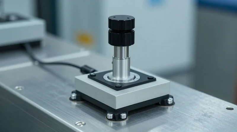
Case Study: Precision Engineering in Sensor Node Deployment
A mid-sized manufacturer of vibration-monitoring sensor nodes for heavy rotating equipment faced a recurring 14-month failure cycle, resulting in significant site-visit costs and operational downtime. By transitioning from a standard 'commodity-grade' assembly process to a mission-critical, precision-optimized PCB manufacturing standard, the firm achieved a 30% increase in mean time between failures (MTBF).
The Engineering Pivot
The optimization focused on three critical areas of the PCB lifecycle: solder joint integrity, conformal coating application, and component sourcing oversight. By implementing these changes, the firm effectively mitigated the environmental stressors prevalent in heavy-industry settings.
| Optimization Area | Original Process | Optimized Process |
|---|---|---|
| Solder Reflow | Standard convection | Nitrogen-purged vapor phase |
| Coating | Hand-sprayed acrylic | Automated robotic silicone |
| Sourcing | Market-price spot buy | Authenticated tiered supply |
ROI Impact Analysis
- What was the primary driver of cost reduction?
The reduction in truck rolls and maintenance man-hours accounted for 70% of the total ROI improvement. - How did PCB optimization influence long-term costs?
Lowering the failure rate reduced the need for periodic total fleet replacements, pushing the amortization schedule from 3 years to over 5 years. - Did manufacturing cost increase?
Yes, unit manufacturing costs rose by 12%, but the subsequent 30% increase in lifespan yielded a net ROI gain of 18% over the sensor's lifecycle.
Material Science and Component Selection for Durability
Engineered Substrates for Thermal Stability
Standard FR-4 substrates often fail to meet the thermal demands of IIoT deployment, where fluctuating temperatures cause mechanical stress via Coefficient of Thermal Expansion (CTE) mismatch. By transitioning to high-Tg (glass transition temperature) laminates or ceramic-filled substrates, manufacturers can ensure structural integrity across extreme temperature cycles, effectively preventing delamination and solder joint fractures.
Comparative Analysis: Substrate Performance
| Material Type | Thermal Performance | Cost-Benefit Profile | Ideal Application |
|---|---|---|---|
| Standard FR-4 | Low/Moderate | Low Initial Cost | Office/Consumer Electronics |
| High-Tg FR-4 | High | Balanced ROI | General Industrial IIoT |
| Polyimide | Excellent | Premium Cost | Aerospace/High-Heat Engines |
Strategic Component Selection and Protection
Beyond the board itself, the lifecycle of a PCB is defined by its ability to resist environmental contamination. Implementing robust conformal coating standards—such as Parylene or silicone-based materials—shields sensitive circuitry from moisture, corrosive gases, and conductive dust. Furthermore, sourcing automotive-grade (AEC-Q100/200) components ensures that individual parts exhibit lower failure rates, significantly reducing the frequency of field maintenance calls.
Frequently Asked Questions
- Does the premium cost of high-Tg substrates yield measurable savings?
Yes. While the bill-of-materials cost increases by 10-15%, the reduction in warranty claims and site-visit maintenance often results in a 30-40% lower Total Cost of Ownership over a five-year deployment cycle. - Which conformal coating offers the best protection against moisture?
Parylene is the industry gold standard due to its chemical inertness and ability to form a pinhole-free, uniform layer, though silicone remains a highly effective, cost-efficient alternative for moderate industrial environments. - Why prioritize AEC-Q rated components in non-automotive IoT?
AEC-Q certification mandates rigorous testing for vibration, thermal shock, and humidity, ensuring that components are built to survive conditions far exceeding standard commercial specifications.
The ROI of Rigorous Quality Assurance (QA) Protocols

In the high-stakes environment of Industrial IoT, the cost of a field failure often exceeds the original manufacturing cost by an order of magnitude. Implementing stringent Quality Assurance (QA) protocols is not merely a compliance checkbox; it is a financial strategy. By deploying Automated Optical Inspection (AOI) and X-ray testing, manufacturers catch microscopic defects—such as solder bridges, cold joints, and voids beneath BGA packages—that would otherwise remain hidden until triggered by thermal cycling or vibration in the field.
Advanced Inspection Technologies: Mitigating Latent Defects
The efficacy of a PCB assembly line rests on its ability to detect failures before shipping. AOI provides rapid, high-resolution visual surface validation, while X-ray inspection is indispensable for modern, high-density interconnections.
| Technology | Primary Target | Impact on ROI |
|---|---|---|
| AOI | Surface defects, missing components, polarity | Reduced scrap and rework costs |
| X-Ray Inspection | Internal solder voids, BGA shorts, hidden connections | Prevention of catastrophic field failures |
Financial Implications of Proactive QA
The return on investment for high-end inspection equipment is realized through the avoidance of 'The Cost of Quality' curve. Identifying a defect at the factory level costs dollars, while fixing a deployed IoT sensor in a remote or hazardous environment costs thousands. By shifting the detection threshold left in the manufacturing cycle, businesses transform QA from a cost center into a risk-mitigation asset.
Frequently Asked Questions
- Why is AOI alone insufficient for modern industrial PCBs?
AOI cannot see through opaque components like BGAs or LGA packages, leaving hidden joints vulnerable to thermal expansion fatigue. - How does X-ray testing specifically improve long-term reliability?
By quantifying solder void percentage, X-ray inspection ensures that joints can withstand the mechanical stress of industrial vibration without cracking. - At what point does advanced inspection become cost-prohibitive?
Inspection becomes cost-prohibitive only when the cost of detection exceeds the predicted cost of field failure multiplied by the probability of occurrence.
Design for Manufacturing (DFM) as a Strategic Asset

Shifting Manufacturing Considerations Upstream
The traditional separation of design and manufacturing roles often leads to 'over-the-wall' engineering, where flaws are only discovered during assembly. By adopting a DFM-centric approach, design teams collaborate with manufacturers during the schematic and layout phases. This integration allows for the identification of potential thermal bottlenecks, assembly hazards, and component sourcing risks before a single prototype is ordered, drastically reducing the necessity for expensive design iterations.
DFM vs. Traditional Design Impact
| Metric | Traditional Design | DFM-Optimized Design |
|---|---|---|
| Prototype Iterations | 3-5 cycles | 1-2 cycles |
| Assembly Failure Rate | High (latent defects) | Low (optimized tolerances) |
| Time-to-Market | Delayed by rework | Accelerated |
| Lifecycle Maintenance | Reactive/Frequent | Proactive/Minimal |
Strategic Reliability and Maintenance Gains
When DFM is applied as a strategic asset, the focus shifts beyond simple 'manufacturability' to 'survivability.' DFM protocols ensure that trace geometries and component spacing are optimized not just for assembly, but for the harsh electromagnetic and mechanical stresses typical of IIoT. This reduces the mechanical fatigue of solder joints and prevents micro-shorts that often plague aging boards, directly lowering field maintenance costs.
Frequently Asked Questions
- How does DFM specifically lower maintenance costs?
DFM identifies high-stress areas during the layout phase, allowing engineers to strengthen trace routing and component anchoring, which reduces the incidence of field failures due to vibration or thermal cycling. - At what stage should DFM reviews begin?
DFM reviews should be integrated into the preliminary design phase, ideally during the initial component selection and board stack-up planning, to avoid costly layout revisions later. - Does early manufacturer collaboration increase initial development time?
While it may add time to the design phase, it significantly reduces the overall project duration by eliminating the 'trial-and-error' cycles that characterize traditional, unoptimized manufacturing hand-offs.
Quantifying the Savings: Maintenance and Replacement Cycles
The Financial Impact of Extended Replacement Cycles
In Industrial IoT deployments, the true cost of a printed circuit board (PCB) is not defined by its procurement price, but by its reliability over a multi-year service life. By investing in optimized manufacturing processes—such as superior thermal management and robust solder joint integrity—organizations can extend the mean time between failures (MTBF). This shift effectively doubles or triples the service interval, fundamentally altering the maintenance budget from reactive, high-cost emergency dispatches to predictable, planned asset management.
Comparing Maintenance Cost Models
| Metric | Standard PCB Design | Optimized Industrial PCB |
|---|---|---|
| Field Failure Rate | High (3-5% Annually) | Low (<0.5% Annually) |
| Replacement Cycle | 2-3 Years | 7-10+ Years |
| Maintenance Expenditure | Reactive/High Cost | Predictable/Low Cost |
Quantifying Maintenance Savings
When calculating ROI, consider the 'Total Cost of Intervention.' This includes not only the cost of the replacement board but the expenses associated with field technician labor, travel time to remote IIoT sites, and the opportunity cost of system downtime. Extending the life of the board by just two years often results in a 40-60% reduction in cumulative maintenance expenditures over a ten-year operational period.
- How does early design optimization influence long-term maintenance?
By designing for thermal dissipation and vibration resistance at the PCB level, you eliminate premature component fatigue, preventing the most common causes of unplanned field failures. - Is the upfront premium for optimized manufacturing worth the investment?
Yes; although high-spec manufacturing may cost 10-15% more initially, it often prevents two or more full-scale replacement cycles over the life of the equipment, providing a significant net positive ROI. - What is the primary indicator of a successful replacement cycle extension?
The primary indicator is a measurable decline in 'Truck Roll' frequency, where maintenance teams no longer need to visit hard-to-access sites to perform emergency repairs on failed control boards.
Future-Proofing Your Industrial IoT Hardware
Selecting a Scalable Manufacturing Partner
The long-term viability of industrial IoT deployments hinges on a manufacturer's ability to maintain rigid quality standards as volumes scale. Partnering with a manufacturer that lacks robust automated infrastructure leads to performance degradation and increased latent defect rates when moving from prototyping to mass production.
| Selection Criteria | Impact on ROI | Maintenance Benefit |
|---|---|---|
| Full-Scale Automation | High consistency; lower per-unit cost | Reduces field failure variance |
| Strategic Component Sourcing | Supply chain resilience | Prevents premature redesign cycles |
| Advanced QA Integration | Lower initial yield waste | Extends device MTBF (Mean Time Between Failures) |
Key Considerations for Future-Proofing
- How does component lifecycle management impact long-term maintenance?
Selecting components with long-term availability prevents costly emergency redesigns and re-certifications, ensuring a stable BOM over the product's entire 10+ year lifecycle. - Why is manufacturing transparency critical?
Deep transparency into the PCB manufacturing process, including traceability records for every batch, allows for proactive issue identification, significantly reducing the scope of expensive field recalls. - Does geographic proximity matter?
While cost-focused strategies often look offshore, choosing partners with advanced logistics or regional hubs reduces the risk of long-term delays in servicing and hardware replacement cycles.
Ultimately, future-proofing is not merely about surviving today's production run; it is about establishing a collaborative framework with your manufacturer. By integrating DFM feedback loops and prioritizing high-grade raw materials early in the cycle, companies can significantly reduce the 'hidden' maintenance costs that frequently erode IoT project profitability.
Prioritizing high-quality PCB assembly is not merely an engineering choice; it is a vital business strategy for reducing technical debt and maximizing hardware ROI. If your team is ready to reduce field failures and extend your deployment lifecycles, contact our engineering experts today to evaluate your current manufacturing standards.
