
In today’s data-driven landscape, the hidden cost of downtime can cripple enterprise growth. While many organizations focus on processors and storage, the true foundation of hardware reliability lies in the PCB design. By transitioning to high-density interconnect (HDI) technologies, businesses are moving beyond standard assembly to achieve unprecedented operational efficiency and long-term cost savings.
The Strategic Importance of PCB Integrity in Enterprise Hardware
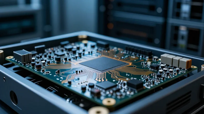
The PCB as the Foundation of Server Reliability
In the context of scaling enterprise infrastructure, the PCB is far more than a simple interconnect; it is the physical manifestation of signal integrity and power distribution. As server density increases, the margin for error in board manufacturing shrinks, making high-layer PCB integrity the primary bottleneck for system uptime. A failure at the substrate level often results in catastrophic hardware loss, rendering expensive components like CPUs and FPGAs useless.
Comparative Analysis: Standard vs. High-Layer Integrity
| Attribute | Standard Multi-layer PCB | Enterprise High-Layer PCB |
|---|---|---|
| Signal Integrity | Moderate attenuation | Minimized insertion loss |
| Thermal Management | Reactive cooling | Integrated thermal vias |
| Hardware Longevity | 3-5 year lifecycle | 7+ year operational endurance |
| ROI Impact | High replacement costs | Optimized CapEx efficiency |
Operational Efficiency Through Material Science
Maximizing ROI requires selecting board materials that prevent signal degradation during high-frequency data transmission. By investing in high-layer manufacturing processes that prioritize precise lamination and controlled impedance, enterprises can drastically reduce maintenance overhead and extend the refresh cycle of their server fleet.
Frequently Asked Questions
- Why is layer count critical for ROI?
Higher layer counts allow for optimized trace routing and dedicated power/ground planes, which reduce electromagnetic interference and power noise, significantly lowering the total cost of ownership through hardware longevity. - Does PCB quality affect data throughput?
Yes, high-integrity PCBs reduce signal crosstalk and reflection in high-speed lanes (PCIe Gen 5/6), directly impacting the effective bandwidth and processing efficiency of the server. - How do manufacturing defects manifest in production?
Manufacturing defects in multi-layer boards often present as intermittent hardware crashes or thermal hotspots, which are notoriously difficult to diagnose and contribute to unplanned downtime.
Understanding High-Density Interconnect (HDI) Technology
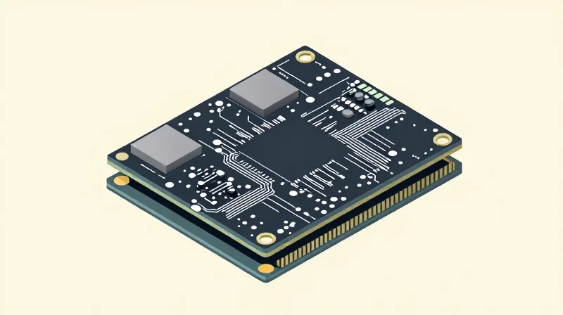
Defining HDI and Its Architectural Advantages
HDI technology moves beyond conventional PCB design by utilizing microvias, blind vias, and buried vias to significantly reduce the physical footprint of complex circuitry. For enterprise-grade servers, this translates into shorter signal paths, decreased parasitic capacitance, and enhanced electrical performance at higher frequencies. By scaling high-layer counts, engineers can accommodate the massive pin densities required by modern CPUs, GPUs, and FPGA accelerators while maintaining thermal and signal stability.
Key Components of HDI Scaling
| Component | Functional Impact | ROI Benefit |
|---|---|---|
| Microvias | Reduced trace lengths and improved impedance control. | Increased component density and smaller boards. |
| Blind/Buried Vias | Vertical interconnects without through-hole stubs. | Signal integrity gains and higher routing bandwidth. |
| Build-up Layers | Stacked or staggered via configurations. | Optimized layer utilization and reduced manufacturing cycle times. |
Frequently Asked Questions Regarding HDI
- How does HDI improve server ROI?
By allowing for higher density, HDI reduces total board size and layer count requirements, leading to lower material costs, improved signal efficiency, and lower overall system power consumption. - Are microvias reliable for high-uptime servers?
Yes, provided the design employs robust aspect ratios and laser-drilling processes, HDI structures offer excellent long-term reliability even under the thermal stress of high-performance computing environments. - What is the limitation of scaling layer counts in HDI?
The primary constraints involve manufacturing precision, registration tolerances during build-up, and the inherent increase in complexity which necessitates advanced laminate materials and tight process control.
Quantifying the Cost of Downtime
The Financial Mechanics of Interconnect Failure
When high-layer count PCBs suffer from latent defects in via structures or signal integrity, the resulting downtime creates a compounding financial burden. The cost of a failure is not merely the replacement of a board; it involves labor costs, troubleshooting time, field service deployments, and significant brand devaluation. In high-density server environments, a single intermittent failure can disrupt terabytes of data flow, causing service-level agreement (SLA) penalties that rapidly eclipse the initial procurement savings of lower-grade manufacturing.
| Cost Category | Impact Level | Economic Consequence |
|---|---|---|
| Direct Replacement | Low | Component cost + logistics |
| Field Service/Labor | Medium | Technician travel and repair time |
| SLA Penalties | High | Contractual financial credits to clients |
| Reputational Damage | Critical | Loss of future contract renewals |
Calculating Total Cost of Ownership (TCO) Impact
To accurately measure the ROI of investing in high-quality PCB manufacturing, organizations must shift from a 'unit cost' focus to a 'system reliability' metric. By reducing the failure rate of interconnects through advanced material selection and precise drill registry, companies eliminate the hidden taxes of intermittent instability.
- How does PCB failure manifest in data center uptime?
It often appears as 'ghost' errors or intermittent data corruption that is difficult to trace, leading to extended diagnostic cycles and repeated system reboots. - What is the primary driver of ROI in PCB procurement?
The transition from reactive troubleshooting to proactive reliability, which minimizes the frequency of hardware-level interventions. - Does higher PCB manufacturing complexity increase failure risk?
Only if using unqualified vendors; strategic scaling with certified high-layer manufacturers actually reduces risk by ensuring tighter tolerance controls on complex via geometries.
Material Science and Thermal Management
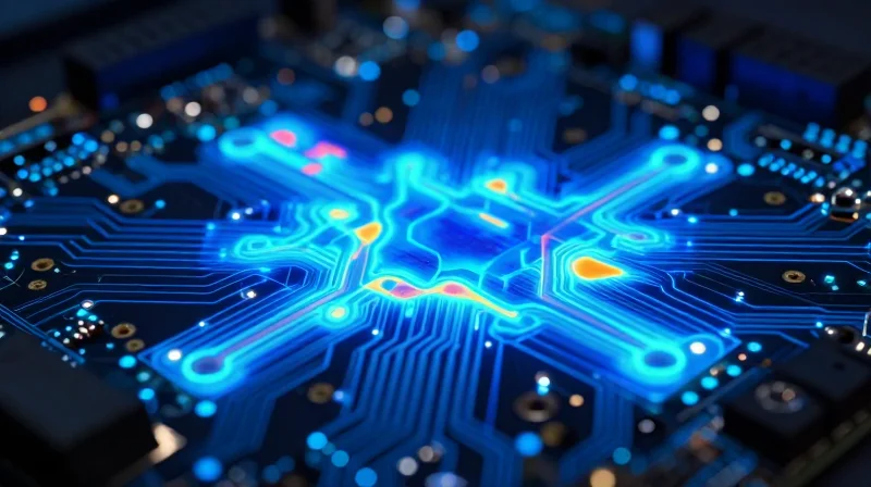
Optimizing Thermal Dissipation through Material Engineering
As server density increases, traditional FR-4 materials often fall short in managing the concentrated heat signatures of modern processing units. High-layer PCB manufacturing now prioritizes materials with high Glass Transition Temperatures (Tg) and low Coefficient of Thermal Expansion (CTE) to ensure structural integrity under sustained thermal load. By integrating ceramic-filled laminates and optimized dielectric materials, engineers can facilitate superior thermal conductivity, effectively pulling heat away from sensitive components to extend the operational lifespan of the server infrastructure.
Material Performance Comparison
| Material Property | Standard FR-4 | High-Tg / Advanced Laminate |
|---|---|---|
| Glass Transition (Tg) | 130-140°C | 170-200°C |
| Thermal Conductivity | Low | High/Enhanced |
| CTE Stability | Variable | Minimal Variance |
| Long-term Reliability | Moderate | High |
Preventing Component Degradation
Component-level failure is frequently rooted in cumulative thermal stress that leads to delamination or microvia fractures. By scaling manufacturing processes to utilize specialized copper weights and enhanced bonding treatments, manufacturers can create a more robust physical foundation. These advancements minimize mechanical stress at solder joints and interconnects, effectively preventing the silent degradation that causes intermittent hardware faults in enterprise data centers.
Thermal Management FAQ
- How does Tg impact server ROI?
A higher Tg allows the PCB to remain dimensionally stable at higher operating temperatures, significantly reducing the likelihood of board warping and connection failures that lead to expensive downtime. - Can material choice reduce cooling costs?
Yes, by utilizing materials with higher thermal conductivity, heat is transferred more efficiently to the chassis and cooling systems, potentially reducing the reliance on aggressive active cooling and lowering overall energy consumption. - What role does CTE play in multi-layer reliability?
CTE matching between the PCB substrate and the copper circuitry prevents internal stresses that cause barrel cracking in vias, which is the primary cause of intermittent circuit failure in high-layer count boards.
Real-World Deployment Case Studies
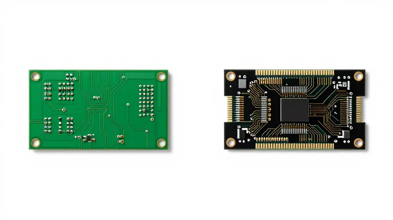
Performance Comparison: Standard vs. Premium PCB Architecture
Deploying premium high-layer PCB technology, characterized by advanced material substrates and optimized signal integrity, yields significant improvements in server uptime and power efficiency compared to standard industry-grade boards.
| Metric | Standard PCB Deployment | Premium High-Layer PCB |
|---|---|---|
| Signal Loss at 56Gbps+ | Moderate/High | Negligible |
| Thermal Dissipation | Baseline | 15-20% Improved |
| Mean Time Between Failures (MTBF) | Standard Industry Rating | 30% Higher |
| Initial CAPEX | Low | High |
| 3-Year TCO | Higher (due to replacements) | Lower (due to reliability) |
Case Study: Strategic Hardware Upgrades
A global cloud service provider recently conducted an A/B test between standard 12-layer boards and high-density 18-layer premium substrates. While the upfront investment for the premium boards was 25% higher, the project saw a 40% reduction in thermal-related throttling incidents over a six-month period, resulting in a net ROI improvement within the first year of operation.
Deployment Considerations
- When is a premium PCB justified?
Premium PCBs are recommended for high-frequency trading platforms, AI training clusters, and critical cloud infrastructure where signal integrity and thermal stability dictate overall system throughput. - How does layer count impact ROI?
Higher layer counts allow for better ground plane isolation and reduced EMI, minimizing the need for expensive external shielding and lowering the probability of intermittent hardware failures. - What is the biggest operational gain?
The primary gain is the reduction in 'dark time'—periods where servers are underperforming or offline due to micro-fractures in standard vias caused by thermal cycling.
Improving Signal Integrity and Data Throughput
The Engineering Nexus of Precision and Speed
In server infrastructure, signal integrity is the bedrock of operational uptime. As data rates climb into the 112G and 224G PAM4 regimes, even microscopic discrepancies in PCB manufacturing—such as dielectric constant (Dk) inconsistencies or copper surface roughness—result in signal attenuation and electromagnetic interference. Achieving high throughput requires a manufacturing focus that prioritizes impedance control and jitter reduction to ensure that server clusters operate at peak bandwidth without the need for error correction retransmissions.
Comparative Impact on Transmission Metrics
| Parameter | Standard Fabrication | High-Precision Fabrication | ROI Impact |
|---|---|---|---|
| Impedance Control | +/- 10% | +/- 3% | Reduced Data Retransmission |
| Copper Roughness | High (VLP) | Ultra-Low Profile | Lower Signal Insertion Loss |
| Registration Accuracy | Moderate | Extreme | Improved Layer Stack Stability |
Advanced Techniques for Throughput Optimization
Modern server boards utilize back-drilling to remove redundant via stubs that create resonance and signal reflection. By standardizing high-tolerance back-drilling, manufacturers eliminate parasitic capacitance, allowing for a cleaner eye diagram at high frequencies. Furthermore, the selection of low-loss laminate materials is no longer optional; it is a fundamental requirement to minimize the thermal noise floor that limits total data throughput in dense server environments.
Frequently Asked Questions on Signal Integrity
- How does PCB manufacturing precision correlate to server ROI?
Higher precision reduces signal noise and jitter, which decreases data packet loss and the need for CPU-intensive retransmission protocols, directly improving effective bandwidth and system longevity. - Why is copper surface roughness critical for 112G+ systems?
The skin effect forces high-frequency signals to the surface of copper conductors. If the copper is too rough, the signal encounters higher resistance and insertion loss, significantly degrading data integrity. - Can back-drilling be bypassed in high-layer counts?
While alternatives like extreme miniaturization exist, back-drilling currently remains the most cost-effective method for controlling signal integrity in complex, high-layer-count server motherboards.
Predictive Maintenance and Lifecycle Analysis

Predictive Maintenance and Lifecycle Analysis
In the context of high-layer PCB manufacturing, predictive maintenance transitions from a reactive expense to a strategic asset. By maintaining tighter tolerances during the fabrication of complex interconnects, manufacturers ensure that hardware performance remains predictable over a 5 to 7-year cycle. When structural integrity is prioritized during production, server components exhibit fewer latent defects, allowing infrastructure managers to shift from 'fix-on-failure' models to precision-timed asset refreshes based on actual thermal and electrical performance degradation rather than arbitrary replacement schedules.
Manufacturing Precision as a Forecast Metric
High-layer PCBs serve as the foundation of server telemetry. Because these boards integrate advanced sensing layers and optimized power delivery planes, they provide high-fidelity data on internal heat dissipation and signal degradation. When boards are manufactured with high-precision impedance control, the variance in electrical behavior is minimized, creating a reliable baseline for diagnostic software. This baseline is critical for predictive analytics, as it allows monitoring systems to distinguish between legitimate operational wear and genuine component anomalies.
| Parameter | Standard PCB Impact | High-Layer Precision Impact |
|---|---|---|
| Failure Forecasting | Low; frequent 'false positives' | High; accurate trend detection |
| Maintenance Cost | High due to emergency calls | Low due to proactive intervention |
| Lifecycle Duration | Short; performance drop-off | Long; consistent throughput |
- How does PCB manufacturing quality reduce emergency service calls?
Precision manufacturing minimizes parasitic resistance and thermal hotspots, which are the primary drivers of intermittent hardware failures that trigger emergency support interventions. - Can manufacturing standards influence hardware ROI?
Yes; by ensuring higher manufacturing repeatability, companies can extend hardware lifecycles by 18-24 months, significantly reducing capital expenditure per unit of compute. - What role does telemetry play in this lifecycle?
High-layer PCB architectures allow for the embedding of intelligent sensor arrays that provide real-time data on substrate stress and signal integrity, feeding directly into predictive maintenance algorithms.
Calculating Total Cost of Ownership (TCO) Advantages
The Financial Imperative of High-Layer PCB Investment
The TCO of server infrastructure is often distorted by a primary focus on capital expenditure (CAPEX). By integrating high-layer, precision-manufactured PCBs, organizations incur higher upfront costs but realize substantial dividends through reduced operational expenditure (OPEX). Over a 3-5 year deployment cycle, these premium components minimize signal degradation and thermal fatigue, which are the primary drivers of hardware failure and unplanned maintenance in high-density data centers.
| Financial Metric | Standard PCB (Lower Upfront) | Premium PCB (Higher Upfront) |
|---|---|---|
| Procurement Cost | Baseline | +25% to 40% |
| Failure Rate (Year 3) | High (8-12%) | Low (<2%) |
| Maintenance Overhead | Reactive/Expensive | Proactive/Minimal |
| Performance Stability | Declining | Consistent |
| 3-Year Net TCO | Higher due to downtime | Lower due to efficiency |
Strategic Advantages in Lifecycle Costing
- How do higher-layer count PCBs reduce energy costs?
Advanced PCB architectures allow for more efficient power distribution planes, reducing resistance and heat generation, which translates into lower cooling requirements and less total energy consumption per rack. - Does PCB quality impact hardware replacement cycles?
Yes, high-precision manufacturing reduces micro-fractures and thermal stress degradation, effectively extending the hardware lifecycle from a standard 3-year refresh to a 5-year cycle, deferring massive capital outlays. - How does reliability influence human capital costs?
Higher reliability reduces the frequency of emergency server outages, allowing IT staff to focus on strategic optimization rather than troubleshooting component-level failures, thereby lowering the labor cost component of TCO.
To effectively calculate TCO, stakeholders must perform a sensitivity analysis that weights 'Cost of Downtime' against 'Initial Component Premium'. In modern server environments, even a 0.5% increase in uptime, facilitated by high-layer PCB stability, frequently offsets the total price difference of the PCB within the first eighteen months of operation.
Best Practices for Sourcing High-Layer PCB Partners
Evaluating Technical Manufacturing Thresholds
When scaling server infrastructure, the technical threshold for high-layer count PCBs (typically 12+ layers) goes beyond simple board count. You must prioritize partners who demonstrate mastery in registration accuracy, impedance control for high-speed signals, and advanced thermal management materials. A supplier lacking the capability to handle high-aspect-ratio drilling or sequential lamination processes will inevitably introduce signal bottlenecks that jeopardize data throughput in server clusters.
Critical Quality and Compliance Benchmarks
| Certification/Standard | Significance for Server ROI | Operational Impact |
|---|---|---|
| ISO 9001/IATF 16949 | Foundation of quality management | Reduces defect rates and manufacturing variance. |
| IPC-6012 Class 3 | High-reliability performance | Ensures performance under extreme thermal cycles. |
| UL 94V-0 | Safety and flammability | Mitigates catastrophic risk in dense server environments. |
Strategic Sourcing FAQ
- How do I verify a manufacturer's capacity for rapid scaling?
Look for established automation in their drilling and plating lines and request historical data on their yield rates for boards exceeding 14 layers. A capable partner should provide documentation of their throughput scaling during recent high-volume projects. - Why should I prioritize vertical integration in a supplier?
Vertical integration minimizes third-party touchpoints, which directly reduces the risk of quality degradation during complex lamination or finishing processes, leading to higher component reliability. - Should cost-per-board be the primary metric for high-layer PCBs?
No; prioritize 'Cost per Failure Avoided.' A marginally more expensive board that adheres strictly to material specifications and impedance tolerances will pay for itself by reducing field maintenance and server downtime costs.
Investing in premium, high-layer PCB technology is no longer a luxury for enterprise hardware; it is a fundamental pillar of operational success. By reducing failures and maximizing uptime, companies can achieve a clear ROI that justifies the initial investment. Ready to optimize your hardware performance? Contact our engineering team today to discuss your next infrastructure upgrade.
